Inspection/Metrology Tools Become the Key Lever for Yield Improvement
As semiconductor manufacturing pushes deeper into advanced nodes, 3D architectures, and heterogeneous integration, yield has become both harder to achieve and more critical to economic success. Traditional levers for yield improvement—recipe tuning, equipment maintenance, and operator experience—are no longer sufficient on their own. Today, inspection and metrology tools have emerged as the key lever for yield enhancement, providing the data, visibility, and control needed to manage processes at nanometer scales and across complex three‑dimensional structures.
This blog post explores why inspection and metrology have moved to the center of yield strategy, how different classes of tools contribute to defect reduction and process optimization, and what this shift means for fabs, equipment vendors, and technology roadmaps.
Yield in the era of extreme complexity
Yield—the fraction of manufactured dies that meet all functional and performance specifications—is a critical determinant of chip cost and profitability. At mature nodes, yield challenges were significant but relatively tractable; defect mechanisms and variability sources were better understood, and feature sizes allowed some margin for process drift.
In advanced logic and memory nodes, feature sizes approach the limits of optical lithography, structures become three‑dimensional, and material stacks grow more intricate. Small variations in critical dimensions, film thickness, or defect density can have outsized impacts on device behavior. Yield losses can occur at any stage, from front‑end patterning and deposition to back‑end assembly and packaging.
In this environment, a fab’s ability to see, measure, and understand its processes in fine detail is the foundation for yield improvement—and that is precisely what inspection and metrology tools deliver.
Inspection vs metrology: complementary roles
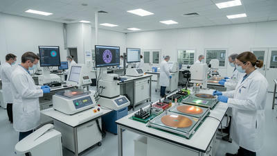
Inspection tools focus on detecting and classifying defects—particles, pattern flaws, contamination, scratches, bridging, and more—across wafers and devices. They answer the question “Where are the defects, and what kinds are they?”
Metrology tools, by contrast, measure process and structural parameters: critical dimensions (CDs), film thickness, composition, roughness, overlay, and topography. They answer “What is the process actually producing, and how close is it to the target?”
Together, inspection and metrology generate the data needed to diagnose yield loss mechanisms, correlate them with specific process steps or tools, and guide corrective actions, making them indispensable to modern yield engineering.
Defect inspection: catching problems before they spread
Defect inspection tools operate at multiple points in the process flow. Front‑end inspection systems examine bare wafers, patterned wafers, and post‑etch surfaces, while back‑end systems check assembly, bumping, and final packaging. Their goal is to detect anomalies early enough that fabs can prevent defective material from consuming further processing and infecting downstream steps.
Brightfield and darkfield optical inspection, along with e‑beam inspection for fine features, allow fabs to identify small particles or pattern defects that might escape visual checks or simple sampling. As nodes shrink, inspection sensitivity must increase without drowning engineers in false positives.
By catching defects promptly, inspection tools help fabs quarantine problem lots, adjust tool conditions, and address root causes before they translate into widespread yield loss or reliability issues in the field.
Critical dimension metrology: controlling the shape of features
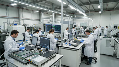
Critical dimensions—line widths, space widths, contact sizes—are fundamental to device performance and variability. CD‑SEM (critical dimension scanning electron microscopes), scatterometry tools, and other metrology platforms measure these features at nanometer precision across the wafer.
At advanced nodes and in multi‑patterning environments, CD control is especially challenging. CD metrology provides feedback on how lithography, etch, and deposition are shaping features, enabling engineers to adjust exposure doses, focus settings, etch chemistries, and other parameters.
Without accurate CD metrology, fabs would be effectively blind to small drifts that can accumulate over time, gradually eroding yield and performance. With it, they gain a powerful lever to keep feature sizes within tight windows, directly supporting higher yields.
Overlay metrology: aligning layers in three dimensions
Overlay—the alignment between successive patterned layers—is critical in devices with many stacked features. Misalignment can cause shorts, opens, or degraded device behavior, and the tolerance for overlay error shrinks at advanced nodes and in 3D structures.
Overlay metrology tools use optical or e‑beam techniques to measure relative layer positions and identify systematic or random alignment errors. Data from overlay measurements feed back into lithography and stage control, helping adjust exposure parameters and mechanical systems.
In logic devices with multiple gate and interconnect layers, and in memory architectures like 3D NAND, overlay precision is a major yield determinant. Robust overlay metrology thus becomes a key lever for ensuring that vertical stacks line up correctly, reducing functional failures and variability.
Film thickness and material metrology: verifying the stack
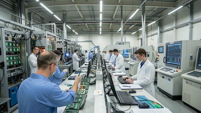
Modern chips rely on complex stacks of materials: high‑k dielectrics, barrier and liner films, low‑k interlayer dielectrics, passivation layers, and more. The thickness and composition of these films must be carefully controlled to achieve desired electrical characteristics and reliability.
Metrology tools such as ellipsometers, X‑ray reflectometers, X‑ray fluorescence systems, and spectroscopic instruments measure film thickness, composition, and uniformity. They help fabs verify that deposition processes (PVD, CVD, ALD) are delivering films within specifications across the wafer and over time.
Accurate film metrology allows fabs to detect drifts in deposition tools, adjust process recipes, and avoid subtle material variations that might cause premature failure or performance spread, supporting higher yield and long‑term reliability.
Inline vs offline metrology: speed and completeness
Inline metrology refers to measurements taken within or directly adjacent to the production line, often on a subset of wafers, with rapid turnaround. Offline metrology involves more detailed, slower measurements in labs or specialized stations. Both have roles in yield improvement.
Inline tools provide quick feedback for day‑to‑day control: adjusting recipes, catching anomalies, and maintaining stability. Offline tools allow deeper investigations into complex issues, such as new defect mechanisms, advanced material analyses, or detailed reliability studies.
Yield strategies increasingly emphasize integrating inline and offline metrology data into unified views, enabling both rapid response and deep understanding. Inspection and metrology tools that bridge these worlds become central to comprehensive yield management.
Data analytics: turning measurements into actionable insights
Inspection and metrology tools produce vast quantities of data—defect maps, CD distributions, overlay vectors, thickness grids, and more. Turning this data into yield improvement requires sophisticated analytics.
Modern fabs use statistical process control (SPC), machine learning, and pattern recognition techniques to identify trends, correlations, and patterns in metrology and inspection data. For example, clustering algorithms can link defect patterns to specific tools or recipes, while regression models can relate CD variations to lithography settings.
As analytics capabilities grow, inspection and metrology tools become even more powerful yield levers: not only do they measure, but their data feeds into intelligent systems that help engineers focus on the most impactful issues and interventions.
Closed‑loop control: automated responses to deviations
Closed‑loop control systems connect metrology and inspection measurements directly to process adjustments. When a tool detects a drift in CD or film thickness, control algorithms can automatically tweak exposure doses, etch times, or deposition rates within pre‑defined limits.
This automation reduces response time and frees engineers from manually correcting every deviation. It also helps maintain processes within tight windows, especially in high‑volume manufacturing where thousands of wafers move through complex toolsets daily.
Inspection and metrology tools that support closed‑loop integration become central to yield, as they are the sensors that drive these control systems, ensuring that corrections are timely and based on accurate data.
Early defect detection and excursion management
Yield excursions—periods when defect rates or variability spike—can be extremely costly if not caught quickly. Inspection tools play a key role in early detection by monitoring defect counts and types across wafers and lots in near real time.
When excursions are detected, fabs can halt processing of affected lots, investigate root causes, and apply corrective actions before large volumes of wafers are compromised. Metrology data helps pinpoint where in the process flow deviations occurred, whether in lithography, etch, deposition, or elsewhere.
This proactive excursion management, driven by inspection and metrology, can save significant material and time, directly improving effective yield and reducing scrap costs.
Back‑end and packaging: yield beyond the wafer
Yield is not determined solely in front‑end processing; back‑end and packaging stages also contribute. Inspection tools check wire bonds, bumps, redistribution layers, and package integrity. Metrology tools measure package warpage, bump height, and other parameters that affect reliability and performance.
As advanced packaging—such as 2.5D interposers, 3D stacking, and chiplets—becomes more common, back‑end inspection and metrology grow in importance. Defects or misalignments in these structures can cause functional failures or limit performance, even if the underlying die is perfect.
Yield strategies increasingly treat front‑end and back‑end inspection/metrology as a continuum, recognizing that overall product yield depends on both chip and package quality, and that data must flow across stages to support holistic improvement.
Capital investment: metrology and inspection as strategic assets
Fabs historically viewed inspection and metrology tools as supporting infrastructure; today, they are seen as strategic assets. Capital expenditure plans allocate increasing budgets to advanced inspection and metrology platforms, recognizing their direct impact on yield and, by extension, profitability.
When choosing where to invest, fabs weigh the expected yield gains from new inspection/metrology capabilities against the cost of tools. In many cases, the economics are compelling: even small improvements in yield at advanced nodes can justify substantial investments in metrology and inspection equipment.
This shift in perception elevates inspection and metrology vendors in the equipment ecosystem and encourages continued innovation in these domains.
Vendor collaboration and co‑development
Inspection and metrology solutions often emerge from close collaboration between tool vendors and fabs. Co‑development projects focus on tailoring tools to specific processes, nodes, and device architectures, adjusting sensitivity, throughput, and measurement capabilities to meet fab needs.
Such collaborations create feedback loops: fabs share yield challenges and data; vendors refine tools and algorithms; new measurements unlock deeper understanding of process behavior. Over time, these partnerships produce highly specialized inspection and metrology solutions that become key differentiators in yield performance.
In this sense, inspection and metrology tools are not generic instruments but co‑crafted components of a fab’s unique yield strategy.
Challenges and trade‑offs: sensitivity, throughput, and cost
Despite their importance, inspection and metrology tools face challenges. Increasing sensitivity can raise false positive rates, overwhelming engineers with non‑critical data. Higher measurement precision often requires slower tools or more complex recipes, impacting throughput.
Fabs must balance sensitivity and throughput, deciding where to apply the most detailed metrology and where sampling is sufficient. They also need to manage the cost of expanding inspection coverage, ensuring that each additional tool or recipe yields a meaningful benefit to yield improvement.
Effective yield strategies therefore treat inspection and metrology as levers to be tuned, not maxed blindly; the goal is to achieve the right level of visibility and control for each process and product mix.
Future directions: AI‑enhanced inspection and virtual metrology
Looking ahead, inspection and metrology are likely to become even more central to yield through AI‑enhanced analysis and virtual metrology techniques. Machine learning models can detect subtle patterns in defect maps and measurement data, predicting yield issues before they fully emerge.
Virtual metrology uses models to infer process parameters from limited physical measurements, effectively extending the reach of metrology tools without measuring every wafer or feature directly. These approaches rely on high‑quality inspection and metrology data for training and validation.
As these technologies mature, inspection and metrology will evolve from passive measurement systems into active intelligence engines that guide process decisions, making them the primary levers for yield improvement in increasingly complex manufacturing environments.
Conclusion: from supporting role to yield cornerstone
Inspection and metrology tools have moved from the background to the forefront of yield strategy. In a world of nanometer‑scale features, 3D structures, and intricate material stacks, they provide the necessary visibility into defects, dimensions, alignment, and material properties.
By enabling early detection, precise control, and data‑driven optimization, these tools have become the key lever for yield improvement. For fabs, investing in and effectively using inspection and metrology is no longer optional—it is central to staying competitive, managing costs, and delivering reliable, high‑performance semiconductor products in the most demanding nodes and architectures yet developed.