Materials

Rising LTA Coverage of Wafer Giants – A Stabilizer for Industry Profitability

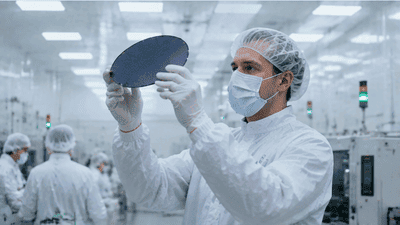
In the complex and cyclical world of semiconductors, stability is a scarce resource. Demand for chips fluctuates with consumer trends, enterprise investments, and macroeconomic swings, while supply chains stretch across continents and multiple tiers of specialized suppliers. Amid this volatility, one segment has become a quiet anchor for industry profitability: the long-term agreements (LTAs) signed between major wafer suppliers and their customers. As LTA coverage rises among wafer giants, it increasingly acts as a stabilizer, smoothing financial performance for both wafer makers and fab operators and reshaping how risk and reward are shared across the value chain.
Qualification Cycles for Domestic Semi Materials Shorten from 24 to 12 Months

In semiconductor manufacturing, material qualification has traditionally been a long and cautious process. For many critical inputs—wafers, gases, wet chemicals, photoresists, CMP consumables, packaging substrates—domestic suppliers often faced qualification cycles of 18–24 months or more before their products could be used in high‑volume lines. Now, in multiple regions, those cycles are shortening, with leading fabs moving toward 12‑month or even sub‑12‑month qualification for carefully selected domestic materials. This shift reflects both greater confidence in local suppliers and strong strategic pressure to accelerate localization without compromising quality or reliability.

SiC Substrate Cost Reduction Curve – Poised to Approach Silicon Levels in 2026

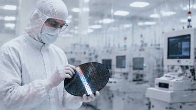
The semiconductor industry is entering a critical transition period as silicon carbide (SiC) technology moves from a specialized material platform toward broader commercial adoption. Once considered an expensive alternative semiconductor material, SiC is rapidly gaining importance in electric vehicles, renewable energy systems, industrial power equipment, and high-efficiency power electronics. A major factor determining the speed of adoption will be the continued decline of SiC substrate costs.

Tracking Expansion Plans of Japan’s Semi Material Giants: Sumitomo, Mitsubishi, Shin-Etsu

Japan’s semiconductor materials sector has long been a quiet powerhouse beneath the global chip industry. From wafers and photoresists to specialty gases, CMP consumables, and packaging materials, Japanese firms anchor critical parts of the supply chain for fabs worldwide. Among these firms, Sumitomo, Mitsubishi, and Shin Etsu stand out as “semi material giants” whose strategies and expansion plans shape both regional ecosystems in Japan and global availability of key inputs.

Critical Localized Components for Gas Delivery Systems

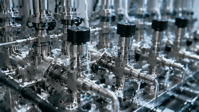
In modern semiconductor fabs, high purity gases are as essential as wafers and photoresists. They feed etch tools, deposition chambers, cleans, and many specialized processes that define device performance and yield. Behind every gas line in the fab is a complex gas delivery system, built from numerous components that must maintain purity, control flow precisely, and ensure safety in an environment where even parts-per-billion contamination can matter. As regions pursue semiconductor localization, attention increasingly turns to “critical localized components” within these gas delivery systems. Localizing these elements is central to building resilient, self-sufficient manufacturing ecosystems.

Volume and Purity Upgrades of Electronic-Grade NaOH in Cleaning Processes

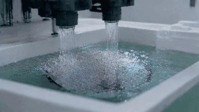
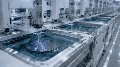
The semiconductor industry is entering a period of unprecedented manufacturing complexity as advanced chips, artificial intelligence processors, automotive semiconductors, and high-performance computing applications continue driving demand for higher-quality production processes. Among the many materials required for semiconductor fabrication, electronic grade sodium hydroxide (NaOH) has become an increasingly important chemical component in wafer cleaning and surface treatment processes.

Wet Chemicals’ Purity Leap from G4 to G5 – Domestic Breakthrough Imminent

In semiconductor manufacturing, wet chemicals are often described as “silent enablers”. They do not appear in headlines like lithography scanners or etch tools, yet they touch almost every wafer in the fab—during cleaning, surface preparation, etching, stripping, and post-CMP processes. As device dimensions shrink and process windows tighten, the purity requirements on these wet chemicals rise dramatically. The industry’s move from G4-grade to G5-grade purity represents not just an incremental improvement in specifications, but a fundamental leap in how chemical supply, analytics, and process integration are conceived. Domestic breakthroughs in achieving and immersing fabs in G5 wet chemical ecosystems are now a key storyline in localization and yield enhancement.

The Irreplaceability and Supply Risks of High-Purity Quartz in Monocrystal Pulling

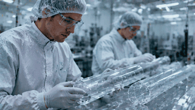
High purity quartz is one of those quietly indispensable materials that sit at the foundation of modern semiconductor manufacturing. In monocrystalline silicon pulling—whether via the Czochralski (CZ) process or related techniques—quartz components shape, contain, and protect the molten silicon from contamination and structural defects. Without reliable access to ultra‑clean quartz crucibles and related parts, the global wafer supply chain would struggle, regardless of how advanced lithography, etch, or deposition tools become.

  • 1
  • 2
  • 3