Materials

Electronic Specialty Gas Usage Surges in Advanced Nodes, Localization Accelerates

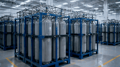
As semiconductor manufacturing pushes deeper into advanced logic and memory nodes, electronic specialty gases have shifted from supporting materials to central enablers of critical processes. Their usage has surged in volume, diversity, and technical importance, particularly in front-end steps such as etch, deposition, doping, and chamber conditioning. At the same time, localization of specialty gas supply—developing domestic or regional production capabilities rather than relying heavily on global imports—has accelerated across multiple semiconductor hubs.
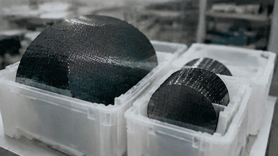
Wafer Size Battle: 300mm Demand Share Continues to Rise, 200mm Stabilizes

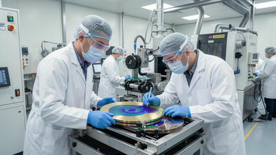
The semiconductor industry has always been defined by continuous technological advancement, and wafer size evolution remains one of the most important drivers of manufacturing efficiency. Over the past two decades, the transition from 200mm wafers to 300mm wafers has reshaped semiconductor production economics by enabling higher output, improved cost efficiency, and greater manufacturing scalability. As global demand for advanced computing, artificial intelligence, automotive electronics, and industrial semiconductors continues to expand, the balance between 300mm and 200mm wafer demand is becoming a critical topic across the semiconductor supply chain.

Photomask Localization Rate Breaks Through – Progress by Qingyi and Luwei

In the semiconductor world, photomasks sit at a critical junction between design data and physical wafers. They encode circuit patterns with nanometer precision and serve as the optical templates for lithography across logic, memory, and specialty devices. For years, high-end photomask capability has been concentrated in a handful of global clusters, making domestic fabs heavily dependent on imported masks for advanced nodes. Recently, however, localization rates in certain regions have begun to break through, driven by progress from emerging players such as Qingyi and Luwei. Their advances mark a significant shift in the balance between global and domestic supply and signal a new phase in the maturation of local semiconductor ecosystems.

Material Inventory Cycles Typically Lead Equipment Inventory by 1-2 Quarters

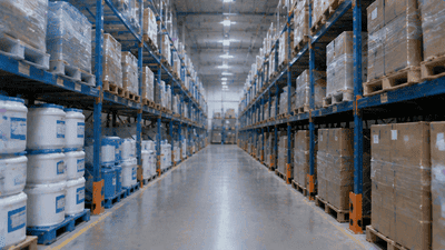
The semiconductor industry operates through one of the most complex supply chains in the global manufacturing ecosystem. From raw materials and specialty chemicals to semiconductor equipment and final chip production, every stage is closely connected through demand signals, inventory adjustments, and capital investment cycles. Understanding the relationship between material inventory cycles and equipment inventory cycles provides important insight into the future direction of semiconductor markets.

Photoresist Supplier Price Hike Wave: Shin-Etsu and JSR’s Strategy Shifts in China

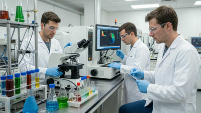
Photoresist sits at the heart of semiconductor manufacturing. As a key material in lithography, it directly shapes how patterns are transferred onto wafers and, ultimately, how advanced devices are made. In recent years, China has emerged as one of the most important semiconductor markets, both as a manufacturing base and as a consumer of critical materials like photoresist. Against this backdrop, a wave of price hikes by major suppliers—and evolving strategy from global leaders such as Shin Etsu and JSR—has become a focal point for fabs, policymakers, and industry observers trying to understand the changing economics of chipmaking in China.

Precursor Demand Explodes in ALD/CVD – Korean Suppliers Dominate

As semiconductor manufacturing races into ever more advanced nodes and complex device architectures, atomic layer deposition (ALD) and chemical vapor deposition (CVD) have become foundational processes for building precision films and 3D structures across logic, memory, and advanced packaging. With this shift, demand for electronic-grade precursors—the reactive molecules that form these films—has exploded. At the same time, Korean chemical and materials companies have steadily expanded their footprint, to the point where they now play a dominant role in supplying key ALD and CVD precursors to global fabs.

Recycling and Circularity of Semi Materials (Green Silicon) as an ESG Investment Theme

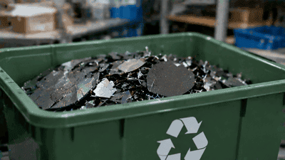
Semiconductor manufacturing sits at the crossroads of technological progress and environmental scrutiny. As demand for chips soars—driven by AI, mobile devices, electric vehicles, and IoT—so do the material flows, energy consumption, and waste streams that underpin fabrication. "Green silicon" and broader circular approaches for semiconductor materials are emerging as crucial elements of environmental, social, and governance (ESG) investment strategies. This article explains why recycling and circulation of semiconductor materials matter, outlines the main technical and market levers, highlights key risks and opportunities for investors, and offers practical frameworks for integrating these themes into ESG-focused portfolios.

Why Semi Material Suppliers Generally Have Higher Gross Margins than Equipment Makers

Within the semiconductor ecosystem, two groups of companies are structurally critical: equipment makers that build the tools used in fabrication, and material suppliers that provide wafers, gases, chemicals, photoresists, targets, and numerous other inputs. Although both operate in demanding, capital‑intensive environments, semi material suppliers typically achieve structurally higher gross margins than equipment manufacturers. This outcome can seem counterintuitive at first glance—tools are expensive and complex—but it makes sense once you examine business models, product lifecycles, and the nature of recurring demand.

  • 1
  • 2
  • 3