
Equipment

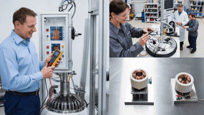
Localization Progress of Equipment Parts: Ceramic Heaters and Electrostatic Chucks

As semiconductor manufacturing becomes more strategically important and supply chains more scrutinized, attention is shifting from headline tools—like lithography scanners and etchers—to the critical parts inside these systems. Among the most important of these parts are ceramic heaters and electrostatic chucks, which play central roles in thermal management and wafer handling in front‑end processes. Their localization, meaning the development and production of these parts within domestic or regional ecosystems rather than relying entirely on imports, is now a key topic for both equipment vendors and fabs.
Consumables Business Model and Valuation Premium of CMP Equipment

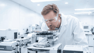
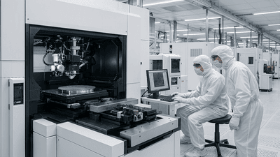
Chemical mechanical planarization (CMP) is one of the quiet but indispensable steps in semiconductor manufacturing, ensuring that wafers remain flat and ready for subsequent patterning and deposition. CMP equipment vendors occupy a distinctive position in the fab tool ecosystem because their business model is tightly linked to consumables—slurries, pads, conditioners, and related materials that must be replenished continuously.

The Decisive Role of Dual-Stage Systems in Lithography Overlay Accuracy

As semiconductor manufacturing has pushed deep into advanced logic and memory nodes, overlay accuracy has become one of the most critical metrics in lithography performance. Overlay—the precise alignment of a new pattern layer to all the layers already on the wafer—directly determines whether transistors, contacts, and interconnects line up within the extremely tight tolerances required at nanometer-scale dimensions. At these nodes, even a few nanometers of misalignment can translate into yield loss, parametric variability, or outright functional failures.

Challenges for Back-End Test Equipment (Probers/Handlers) in Massive AI Chips

Massive AI chips—large, power‑hungry accelerators packed with billions of transistors and complex interconnect fabrics—have rapidly become central to data centers, cloud platforms, and high‑performance computing systems. Their front‑end design and fabrication attract much attention, but back end test is just as critical. Probing and handling these devices at wafer sort and final test is significantly more challenging than for traditional logic or consumer chips, because AI devices push the limits of size, power, thermal behavior, and interface complexity.

ALD Usage Doubles in Advanced Process Nodes

Atomic layer deposition (ALD) has moved from a niche technique to a central pillar of thin-film engineering in leading-edge semiconductor manufacturing. As process nodes advance into ever smaller geometries and more complex three-dimensional architectures, fabs are turning to ALD far more frequently than in previous generations. The statement that “ALD usage doubles in advanced process nodes” captures a real and powerful trend: each node shrink and structural transition typically brings a step-change in how often, and how critically, ALD is used across the flow.

2026 Global Semi Equipment Market Forecasts: A Summary of Institutional Divergence

The 2026 global semiconductor equipment market sits at the intersection of multiple, sometimes conflicting forces: post-downturn recovery, structural demand from AI and automotive, technology transitions at advanced nodes, and ongoing geopolitical constraints. Institutions that track and forecast this market—industry associations, research houses, banks, and policy bodies—do not agree on a single trajectory. Instead, their forecasts diverge along several axes: size of the rebound from recent softness, sustainability of capital expenditure cycles, and the regional composition of spending.

Edge Polishing Equipment Opportunities in Growing SOI Substrate Demand

Silicon-on-insulator (SOI) substrates have moved from a niche technology into a mainstream enabler for high‑performance, low‑power, and high‑voltage semiconductor devices. As adoption expands in RF, automotive, power management, and advanced logic applications, demand for SOI wafers is rising steadily. This growth is not just about the active silicon layer and buried oxide quality; it also places new emphasis on wafer edge characteristics, opening a distinct opportunity space for specialized edge polishing equipment.

Shortage Cycles of Semi Equipment Components (RF Generators, Vacuum Pumps, Ceramics)

Semiconductor equipment may command the headlines, but behind every etcher, deposition tool, or plasma cleaner sits a network of critical components that quietly determine whether fabs can actually run at full capacity. RF generators and matching networks power plasmas, vacuum pumps sustain clean low‑pressure environments, and ceramic parts protect chambers while withstanding extreme conditions. When these components fall into shortage, the impact cascades through tool delivery schedules, fab utilization, and ultimately chip supply.

  • 1
  • 2
  • 3