Equipment

Coat/Develop Equipment Localization Rate First Breaking 30% – Industry Significance

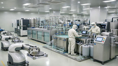
The lithography track—specifically coat and develop equipment—has long been one of the most strategically sensitive segments of semiconductor manufacturing. For years, a small number of global suppliers dominated this space, providing the photoresist coating and developing tools that sit directly alongside lithography scanners and define patterning quality and throughput. The news that localization rates for coat/develop equipment have, for the first time, broken through the 30% threshold is therefore more than a statistical milestone. It represents a meaningful shift in technological capability, supply‑chain security, and bargaining power across the industry.
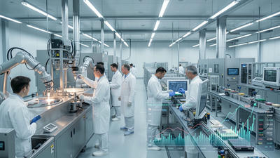

2026 Semi Equipment Localization Targets and Their Capital Market Reflections

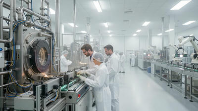
Semiconductor equipment localization moved from a long‑term aspiration to an explicit 2026 policy target in many key manufacturing regions. Governments and industry coalitions have set concrete goals for the share of critical tools—lithography tracks, etch and deposition systems, metrology instruments, back‑end and packaging equipment—that should be sourced from domestic or regional suppliers. These targets are not only reshaping procurement strategies inside fabs; they are also sending clear signals to capital markets, where investors sift through winners and losers in the emerging localized equipment ecosystem.

Advanced Packaging Equipment Growth Outpaces Front-End Equipment for the First Time

For decades, the center of gravity in semiconductor capital spending has lived squarely in the front end of the line—lithography, etch, deposition, and other wafer‑fab tools. Packaging was often treated as an afterthought: necessary, but secondary. That hierarchy is now changing. For the first time, growth in advanced packaging equipment is outpacing growth in traditional front end equipment, signaling a structural shift in how performance, cost, and innovation are created in the chip industry.

2026 Breakthroughs in Lithography Supply Chain Localization: A Critical Component Progress List

In 2026, efforts to localize the lithography supply chain—once seen as an almost impossible task—have begun to show tangible progress. Lithography, the core process technology enabling advanced semiconductors, has long depended on a small set of suppliers for key tools and materials. This concentration created geopolitical vulnerability, bottlenecks, and strategic concerns for countries and regions that rely heavily on imported equipment and components. Over the past year, multiple initiatives have focused on building domestic capabilities and diversifying sources for critical lithography inputs.

The Critical Role of Etching Equipment in 3D NAND’s 500-Layer Breakthrough

The push toward 500‑layer 3D NAND marks one of the most ambitious feats in modern semiconductor manufacturing. As vendors stack more layers to drive bit density and lower cost per bit, the process challenges grow exponentially rather than linearly. At the center of these challenges sits etching equipment. While lithography and deposition often capture headlines, it is the precision, selectivity, and reliability of advanced etchers that make ultra‑tall vertical structures physically realizable at scale. Without breakthroughs in etching technology, a 500‑layer architecture would remain a simulation rather than a shipping product.

Global Wafer Shipment Area Stabilizes and Rebounds – Equipment Inflection Confirmed

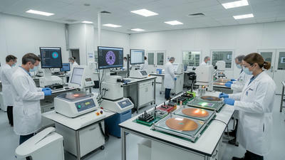
After several volatile years in the semiconductor cycle, global wafer shipment area has finally moved from contraction to stabilization and, more recently, to a clear rebound. This turning point is more than a statistical curiosity: it signals a broad‑based recovery in chip demand and a renewed appetite for equipment investment. As wafer area shipped stabilizes and then climbs, the reflection in front‑end manufacturing equipment orders and utilization is becoming unmistakable, confirming that the industry has entered a new phase of expansion.

Equipment Makers Transition from Hardware Sales to "Hardware + Service + Consumables" Model

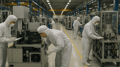
Semiconductor manufacturing has long been defined by massive capital investments in complex tools: lithography scanners, etchers, deposition systems, implant machines, metrology platforms, and packaging equipment. For decades, the core business of most equipment makers revolved around selling this hardware—large, one‑time transactions that anchored fab capacity expansion and technology upgrades. Today, that model is undergoing a decisive transformation. Across the industry, equipment makers are shifting from pure hardware sales toward integrated “Hardware+Service+Consumables” offerings, where long‑term support contracts, process services, and recurring consumable sales form an increasingly large share of revenue and strategic focus.

Wet Cleaning Tools’ Share of Process Steps Continues to Rise in Advanced Nodes

As semiconductor manufacturing has pushed into ever more advanced nodes, wafer cleaning has evolved from a supporting operation into one of the central pillars of yield and device performance. At leading logic and memory nodes, the share of total process steps devoted to cleaning tools—single-wafer cleans, batch cleans, bevel cleans, and specialized surface treatments—continues to rise. This expansion reflects a simple reality: smaller geometries, complex three-dimensional structures, and new materials leave far less margin for particles, residues, and surface defects, making cleaning an indispensable, frequently repeated step throughout the flow.

  • 1
  • 2
  • 3