

Equipment

2026’s Biggest Variable for Equipment Localization: Complete Lithography System Progress

In semiconductor manufacturing, “equipment localization” has become a central strategic goal for many countries: building domestic or closely allied capability to produce and maintain the tools that make chips. Across etch, deposition, cleaning, test, and packaging, notable progress has been made. Yet in 2026, one segment still stands out as the biggest variable in localization efforts: complete lithography systems. Lithography remains the technical and strategic bottleneck, and the pace of progress toward localized, fully integrated lithography platforms will largely determine how far and how fast equipment localization can go.
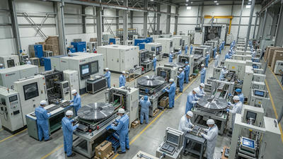

The Leap from 20% to 50% Localization – Ranking the Beneficiaries Across Segments

Semiconductor localization has moved from abstract policy talk to concrete numerical targets. Many countries and regions now speak explicitly about raising the local share of their semiconductor value chain—from 20% toward 50% or more—across materials, equipment, design, and manufacturing. This leap is not incremental; it fundamentally changes how risks, costs, and strategic advantages are distributed in the ecosystem.

Oligopoly Structure of the Ion Implanter Market and China’s Breakthrough Opportunities

Ion implanters sit at the core of modern semiconductor manufacturing, enabling precise doping of silicon and other substrates to form the active regions of transistors and memory cells. Over decades, this highly specialized equipment segment has evolved into a tight oligopoly dominated by a handful of global vendors with deep process know‑how, sophisticated engineering capabilities, and entrenched customer relationships. For new entrants, especially those in emerging technology powers like China, this structure presents both formidable barriers and compelling strategic opportunities.

Thin Film Deposition Tools (PVD/CVD/ALD) See Surging Demand, Orders Booked into 2027

Thin film deposition sits at the core of modern semiconductor manufacturing, quietly shaping every transistor, interconnect, and memory cell. As chips become more complex and vertically integrated, the demand for high‑performance deposition equipment—especially physical vapor deposition (PVD), chemical vapor deposition (CVD), and atomic layer deposition (ALD)—has accelerated. In recent cycles, this demand has reached the point where order books for key tools are being filled well into 2027, signaling both a structural shift in capital expenditure and a sustained confidence in long‑term semiconductor growth.

Assessing the Impact of 2026 New US Export Controls on Equipment to China

The semiconductor industry entered 2026 already shaped by several years of tightening technology and trade restrictions, and new US export controls on equipment shipments to China add another layer of complexity. These measures aim to constrain China’s access to advanced manufacturing capabilities, particularly for leading‑edge logic, memory, and certain specialty devices that have strategic or military relevance. For companies operating fabs, supplying tools, or sourcing equipment in China, the question is not whether these controls matter—they clearly do—but how their impact will differ across segments, time horizons, and strategic options.

Booming Used Equipment Market – An Alternative Path for Mature Node Capacity Expansion

As global demand for semiconductors at mature process nodes continues to grow, chipmakers face a strategic question: how to expand capacity without committing to the full cost and lead time of brand‑new fab tooling. In this environment, the used semiconductor equipment market has shifted from a niche corner of the industry into a booming, mainstream alternative. Buying, refurbishing, and redeploying used tools has become a key path for adding mature node capacity quickly and economically, reshaping investment decisions and competitive dynamics across the ecosystem.

Rising Penetration of Equipment Leasing Models Among China’s Small-to-Mid Fabs

Small and mid‑sized semiconductor fabs in China are under intense pressure to expand capacity, upgrade technology, and remain competitive, all while facing tight capital budgets and a rapidly changing market landscape. The traditional model of buying expensive front‑end and back‑end equipment outright is increasingly difficult to sustain for these fabs, especially when technology lifecycles are shortening and demand cycles remain volatile. In this environment, equipment leasing and related flexible acquisition models are gaining traction as practical solutions.

A Side-by-Side Comparison of 2026 Guidance from ASML, AMAT, LRCX, and TEL

Guidance for 2026 from the four global leaders in semiconductor equipment—ASML, Applied Materials (AMAT), Lam Research (LRCX), and Tokyo Electron (TEL)—offers a window into how each is positioned for the next phase of the wafer fab and advanced packaging cycle. While the numerical details differ, the guidance sets share common themes: strong demand tied to AI and advanced nodes, resilient spending on mature and specialty technologies, and varying degrees of caution around geopolitics and export controls.

  • 1
  • 2
  • 3