Wet Cleaning Tools’ Share of Process Steps Continues to Rise in Advanced Nodes
As semiconductor manufacturing has pushed into ever more advanced nodes, wafer cleaning has evolved from a supporting operation into one of the central pillars of yield and device performance. At leading logic and memory nodes, the share of total process steps devoted to cleaning tools—single-wafer cleans, batch cleans, bevel cleans, and specialized surface treatments—continues to rise. This expansion reflects a simple reality: smaller geometries, complex three-dimensional structures, and new materials leave far less margin for particles, residues, and surface defects, making cleaning an indispensable, frequently repeated step throughout the flow.
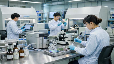
This blog post explores why wafer cleaning tools are taking a larger share of process steps in advanced nodes, how different cleaning approaches map onto critical process modules, what this means for tool suppliers and fabs, and how cleaning technology is evolving alongside patterning, deposition, and etch. The goal is to show that cleaning is no longer just “preparation” or “finishing” but an active, continuous enabler of next-generation semiconductor manufacturing.
From supporting role to central process module
In earlier generations of semiconductor manufacturing, cleaning steps primarily served as preparation and post-process operations: removing particles from incoming wafers, stripping photoresist after lithography, or clearing residues from etch and deposition. While important, they often accounted for a relatively modest share of total process steps compared with lithography, etch, implantation, and deposition.
At advanced nodes, that balance has changed. Shrinking critical dimensions, tighter overlay tolerances, and more complex stacks mean that any contamination or residue can cause defects, line edge roughness, pattern collapse, or reliability failures. As a result, fabs insert more cleaning steps before and after critical processes, and they rely on cleaning tools to manage interfaces between materials that were rarely seen in older nodes.
This shift is visible in process flows where cleaning steps now punctuate almost every major module—patterning, etch, deposition, CMP, and even packaging—signaling a new level of prominence for cleaning tools.
Advanced nodes amplify sensitivity to contamination
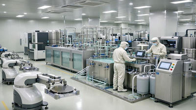
The primary driver behind the rising share of cleaning steps is sensitivity. At advanced nodes, feature sizes approach dimensions where single particles or nanometer-scale residues can disrupt entire structures. A small particle in a narrow trench can block subsequent deposition or cause voids; a thin residue layer on a critical interface can change electrical properties or induce reliability issues.
Moreover, surface chemistry and roughness become more important. As devices rely on high-k dielectrics, complex metal stacks, and engineered interfaces, the condition of surfaces before each deposition or etch step strongly affects film nucleation, adhesion, and uniformity. Cleaning tools are responsible for setting those initial conditions, not just removing obvious contaminants.
Because of this heightened sensitivity, fabs treat cleaning as a precision process that underpins yield, rather than a generic “washing” operation that can tolerate variability.
More materials, more interfaces, more cleans
Advanced logic and memory nodes introduce more materials: multiple dielectrics, barrier layers, liners, metals, nitrides, oxides, and exotic compounds. Each material interface presents its own challenges—native oxides, residual chemistries from prior steps, and surface states that can affect subsequent reactions.
Cleaning tools must be tailored to these interfaces. A chemistry that works well on one material may damage another or leave residues that interfere with downstream processes. As material diversity increases, process engineers divide cleaning into finer-grained steps, each tuned for a specific stack or interface, instead of relying on a small set of generic cleans.
The result is a growing number of cleaning recipes and insertions, expanding the share of total process steps dedicated to cleaning operations throughout the wafer’s journey.
Single-wafer cleaning: precision and flexibility
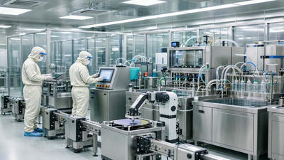
Single-wafer cleaning tools have seen particularly strong growth in advanced nodes. Unlike batch tanks, single-wafer systems can deliver highly controlled chemistries, flow patterns, and mechanical actions (such as megasonic agitation or spray/brush) to each wafer individually.
This precision is crucial when dealing with delicate features, narrow spaces, and sensitive materials. Single-wafer cleans can target specific residues while minimizing damage to underlying structures, and they can incorporate multi-step sequences in a single chamber or tool cluster. Recipes can be tuned to different layers within a node, providing flexibility as device designs evolve.
As a consequence, single-wafer cleaning tools increasingly occupy more slots in front-end-of-line (FEOL) and middle-of-line (MOL) toolsets, and they account for a growing share of the total clean steps in those modules.
Batch and tank cleans still matter—but differently
Batch cleaning tools, such as wet benches and tank systems, remain deeply embedded in semiconductor fabs, especially for certain legacy processes, bulk cleans, and high-throughput operations. In advanced nodes, their role shifts toward specific stages where large numbers of wafers require similar treatments and the risk of feature damage is lower.
For example, batch cleans may handle initial wafer preparation, gross contamination removal, or certain post-CMP cleans where the features are robust enough to withstand generic chemistries and immersion cycles. These steps can still be numerous, and they contribute to the overall count of cleaning processes.
However, as nodes advance, batch cleans are complemented—not replaced—by more targeted single-wafer or modular cleans, which increases the total variety and frequency of cleaning operations across the line.
Patterning and lithography: cleaning before and after
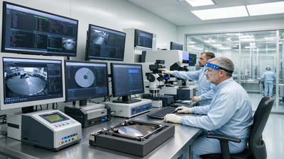
In advanced patterning flows, especially those involving multiple patterning, EUV lithography, or complex resist stacks, cleaning steps bracket lithography operations. Before exposure, wafers undergo cleans to ensure surface uniformity, control residual films, and remove particles that could cause defects or focus variations. After exposure and development, cleans remove residual resist or scum and prepare surfaces for subsequent etch.
In multi-patterning schemes, these sequences repeat several times across a single layer, multiplying the number of cleaning steps associated with lithography. Cleaning tools designed specifically for resist and post-develop residues therefore see more use as nodes shrink.
This patterning-linked expansion is a major factor in the rising share of cleaning operations, especially in logic nodes where critical layers demand tight control over line profiles and roughness.
Etch and deposition: cleans for interface preparation
Etch and deposition modules also rely heavily on cleaning tools. Before etching, surface preparation cleans can remove native oxides, adjust surface chemistry, or strip unwanted films that might interfere with etch selectivity or profile control. After etch, post-etch cleans remove residues, polymers, and redeposited materials that accumulate during plasma exposure.
Similarly, deposition processes such as CVD, ALD, and PVD require clean surfaces to achieve uniform nucleation and dense, defect-free films. Pre-deposition cleans can include oxide removal, surface functionalization, and particle clearing tailored to the specific film to be deposited. Post-deposition cleans may address unwanted sidewall deposits or residual precursors.
As more layers and finer features are introduced in advanced nodes, the number of etch and deposition steps rises—and with them, the number of associated cleans. Cleaning tools thus become integral components of each module rather than occasional, standalone operations.
CMP and planarization: cleaning as a companion
Chemical mechanical planarization (CMP) is crucial for achieving flat surfaces in multilevel interconnects and complex stacks. CMP inherently generates slurry residues, particles, and potential surface contamination that must be removed promptly to avoid defects and cross-contamination.
Post-CMP cleaning steps, often performed on dedicated tools, aim to remove slurry particles, pad debris, and chemical residues without damaging the polished films. As interconnect stacks grow more complex and CMP steps increase in number, the associated cleaning operations expand in lockstep.
This coupling between CMP and cleaning adds another dimension to the rising share of cleaning tools in advanced-node process flows.
3D architectures: more surfaces, more cleans
Three-dimensional architectures such as FinFETs, gate-all-around nanosheets, and 3D NAND introduce surfaces that are harder to reach and more sensitive to contamination. Vertical channels, sidewalls, and buried interfaces can trap residues or particles that are difficult to remove using traditional methods.
Cleaning tools must adapt with tailored chemistries, flow patterns, and mechanical actions that can access these complex geometries without causing feature collapse or erosion. Additional cleans may be inserted specifically to address 3D features—for example, specialized cleans for deep trenches or vertical stacks.
As 3D architectures become dominant in advanced nodes, the complexity and number of required cleaning steps rise accordingly, further boosting the overall share of cleaning processes in manufacturing.
Defect control and yield: cleaning as a key lever
Yield optimization at advanced nodes increasingly focuses on defect control, including particles, pattern defects, and interface-related issues. Cleaning tools are one of the main levers for reducing defectivity by controlling particulate contamination and chemical residues at each critical step.
Process engineers analyze defect maps and inline inspection data to identify where cleaning steps can be added or modified to reduce specific defect types. For example, a particular particle cluster may be traced to a post-etch residue that can be mitigated with a more aggressive or tailored clean. As these interventions accumulate, the count of distinct cleaning steps grows.
In this sense, the rising share of cleaning tools reflects conscious yield engineering, where cleaning is used strategically as part of defect reduction programs rather than being treated as a generic, fixed module.
Tool design evolution: more cleaning capability per footprint
As cleaning processes multiply, equipment vendors have responded by designing more capable and compact cleaning tools. Multi-chamber systems, modular platforms, and integrated cluster tools allow multiple cleaning recipes to be executed within a single footprint, reducing wafer handling and cycle times.
Tools may combine megasonic cleaning, spray or jet processes, chemical immersion, and drying in programmable sequences, enabling flexible insertion of cleans throughout the flow. Integration with metrology and inspection tools can provide feedback on cleaning effectiveness, informing recipe adjustments and further optimization.
This design evolution supports the growth in cleaning step share without necessarily expanding fab floor space proportionally, making cleaning more pervasive yet manageable within existing facility constraints.
Process integration: cleaning as a design parameter
In advanced nodes, cleaning is considered during process integration from the outset. Engineers design modules—such as gate stack formation, contact etch, or interconnect patterning—with explicit cleaning steps included between operations, rather than adding cleans only when problems arise.
This proactive approach treats cleaning as a design parameter: its chemistry, mechanical action, and timing are chosen to complement etch and deposition conditions, material properties, and device requirements. As integration schemes become more sophisticated, the number of planned cleaning steps naturally increases.
Cleaning thus becomes woven into the fabric of process integration, rather than being an external patch on existing flows.
Implications for tool suppliers and business models
The rising share of cleaning steps creates both growth and competitive pressure for tool suppliers. On the one hand, demand for advanced cleaning equipment—particularly single-wafer and highly configurable systems—expands as fabs add more cleaning modules. On the other hand, competition intensifies as vendors seek to differentiate through performance, reliability, cost of ownership, and integration capabilities.
Tool suppliers may offer new business models, such as performance-based service contracts, modular upgrades, or integrated process solutions that include cleaning, etch, and deposition recipes tuned together. Cleaning tools are no longer sold only as hardware; they are packaged with chemistry partnerships, data analytics, and application support that address specific advanced-node challenges.
This evolution underscores how central cleaning has become to overall fab strategy, affecting not only process flows but also supplier relationships and cost structures.
Environmental and safety considerations
More cleaning steps mean greater use of chemicals, water, and energy, raising environmental and safety considerations. Advanced fabs must manage chemical consumption, waste treatment, and worker safety in the context of an expanded cleaning footprint.
Cleaning tool technology is responding with more efficient chemistries, reduced chemical volumes, improved recycling systems, and designs that minimize emissions and exposure. Dry or low-liquid cleans, alternative chemistries, and better containment and exhaust systems help balance process demands with sustainability goals.
In advanced nodes, environmental performance becomes another axis of cleaning tool differentiation, alongside yield, throughput, and cost of ownership.
Looking ahead: cleaning’s role in future nodes
As the industry looks beyond current advanced nodes to even smaller geometries, more intricate 3D structures, and heterogeneous integration, the trajectory of cleaning’s rising share is unlikely to reverse. New device architectures, such as chiplets and advanced packaging schemes, introduce additional surfaces and interfaces that require careful preparation and residue management.
Emerging processes—like selective deposition, area-selective etch, and new materials for interconnects or memory—will bring new cleaning challenges that demand innovative chemistries and tool capabilities. Process designers may use cleaning steps not only to remove unwanted matter but also to actively tune surfaces for selective reactions, further blurring the line between “cleaning” and “surface engineering.”
In this future, cleaning tools will remain central to enabling yield and performance, and their share of process steps may continue to climb as fabs pursue increasingly ambitious device designs.
Conclusion: cleaning as a cornerstone of advanced manufacturing
The increasing share of wafer cleaning tools in advanced-node process steps is a natural consequence of the industry’s push toward smaller, more complex, and more demanding semiconductor devices. Cleaning now underpins nearly every major module—patterning, etch, deposition, CMP, and beyond—serving as a key determinant of yield, reliability, and performance.
For fabs and tool suppliers, recognizing cleaning as a cornerstone rather than a peripheral operation is essential. Investing in advanced cleaning technology, integrating it thoughtfully into process flows, and continuously optimizing recipes for new materials and structures will remain fundamental to success at current and future advanced nodes.