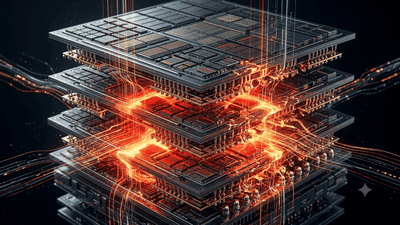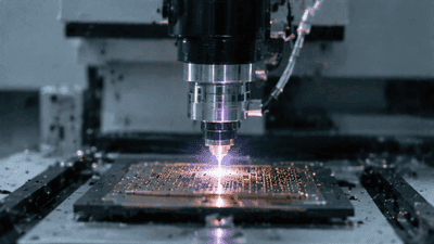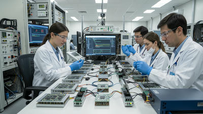
New Applications of High-Energy Ion Implantation in SiC Power Devices
Silicon carbide (SiC) has become one of the most important wide bandgap semiconductors for next‑generation power electronics, thanks to its ability to handle high voltages, high temperatures, and fast switching with relatively low losses. As SiC devices move deeper into electric vehicles, renewable energy systems, industrial drives, and data center power supplies, process technologies around SiC must evolve to unlock the full potential of the material. High energy ion implantation is one of those enabling technologies, and its role is expanding beyond conventional doping to a wider range of applications within SiC power devices.
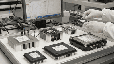
This blog post discusses how high energy ion implantation is used in SiC manufacturing today, why it is particularly well suited to the material’s physical properties, and what new applications are emerging as device architectures and performance targets become more demanding. It focuses on power MOSFETs, diodes, and advanced structures, and outlines how process engineers can leverage high energy implants to create more efficient, robust, and compact power solutions.
SiC power devices: context for implantation
SiC power devices, such as MOSFETs, Schottky diodes, and junction barrier Schottky (JBS) diodes, differ from their silicon counterparts in several key ways. The wider bandgap and higher critical electric field allow thinner drift layers for the same blocking voltage, reducing on‑resistance and enabling higher efficiency. SiC also has superior thermal conductivity and can operate at elevated junction temperatures, which simplifies thermal management and supports high‑power, high‑frequency applications.
To realize these benefits, however, device manufacturers must control doping profiles with great precision. Junction depths, lateral doping gradients, and compensation layers all play critical roles in determining breakdown voltage, on‑state losses, switching behavior, and reliability. High energy ion implantation is a powerful tool in this context, because it can introduce dopants deep into the SiC structure with controllable concentration and spatial distribution.
As device designs evolve to higher voltages, more complex field‑management schemes, and compact layouts, the need for sophisticated implant strategies naturally increases.
Why high energy ion implantation matters in SiC
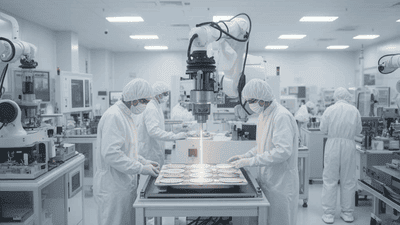
In SiC, dopant diffusion is extremely limited compared to silicon. This means that traditional thermal diffusion techniques, which are widely used in silicon devices, are not effective for forming deeper or tailored junctions in SiC. Ion implantation becomes the primary method for introducing dopants such as nitrogen, aluminum, and others into specific regions of the device.
High energy implantation extends the reach of this method. While low‑to‑medium energy implants are suitable for shallow regions near the surface, high energy implants penetrate deeper into the SiC lattice, enabling the creation of buried layers, deep wells, and tailored vertical profiles. For high‑voltage devices, these capabilities are essential: controlling the internal electric field distribution often requires carefully placed deep doping regions that cannot be formed by surface‑limited processes.
In short, high energy ion implantation gives process engineers a way to shape the internal landscape of SiC power devices with fine control, even in the absence of significant dopant diffusion during subsequent thermal treatments.
Traditional uses of ion implantation in SiC devices
Before exploring new applications, it is useful to recall how ion implantation is traditionally used in SiC power device flows. Common uses include the formation of source and body regions in SiC MOSFETs, defining p‑type regions in JBS diodes, and creating guard rings or termination structures around device perimeters.
These implants are often performed at moderate energies, targeting depths appropriate for surface‑proximate features. They are followed by high‑temperature anneals to activate the dopants and repair lattice damage caused by implantation. Over time, equipment and recipes have improved to balance activation efficiency, defect reduction, and device performance.
High energy variants of these processes have been used when deeper junctions or more complex termination structures are required, but historically they might have represented a smaller fraction of the overall implant budget. That balance is now changing as device architectures become more advanced.
Deep junction formation for high‑voltage MOSFETs
One major new application of high energy ion implantation in SiC is the formation of deep junctions for high‑voltage MOSFETs. As designers aim for devices that can block increasingly high voltages while maintaining low on‑resistance and fast switching, they often introduce deep p‑type or n‑type regions that shape the electric field in the drift region and at the device edges.
High energy implants allow these regions to be formed without relying on thick epitaxial layers with uniform doping. Instead, process engineers can implant carefully controlled deep wells to create field plates, shield regions, or tailored junction profiles. This can improve breakdown voltage, reduce field crowding near critical interfaces, and enable more compact device layouts.
For example, deep p‑type implants beneath the channel or drift region can help manage charge balance and improve short‑circuit robustness, while deep n‑type implants can define buried layers that interact with surface structures to control the voltage distribution during off‑state operation.
Advanced edge termination and field‑management structures
Edge termination is a crucial element in high‑voltage power devices, preventing premature breakdown at the device edges where electric fields can concentrate. Common techniques include guard rings, field plates, and junction termination extensions. In SiC, the high critical field and thinner drift regions make termination design even more sensitive.
High energy ion implantation enables more sophisticated edge termination schemes by creating deep, graded doping profiles near the device perimeter. Multiple high energy implants with varying doses and energies can produce a controlled lateral and vertical charge distribution that spreads the electric field more evenly during high‑voltage operation.
These advanced termination structures can increase breakdown voltage, reduce leakage, and improve robustness under surge conditions. They also allow designers to shrink the termination area, increasing effective device area per wafer and improving cost‑efficiency without compromising reliability.
Buried layers for charge compensation and superjunction‑like concepts

Charge compensation is a powerful concept in power device design, often associated with superjunction structures in silicon. The basic idea is to balance p‑type and n‑type charges in the drift region so that the device can support a high blocking voltage with lower on‑resistance than a uniformly doped drift layer.
In SiC, achieving superjunction‑like performance is challenging because of process and material constraints, but high energy ion implantation opens pathways to approximate or realize similar ideas. By implanting deep, alternating or carefully positioned doped regions, process engineers can create buried layers that participate in charge compensation.
These buried structures may not be identical to classic superjunction columns, but they can provide partial charge balancing effects that improve the trade‑off between on‑state resistance and breakdown voltage. High energy implantation is essential here because the compensating regions must extend through much of the drift thickness, which is difficult to achieve with shallow implants alone.
Tailored vertical profiles in drift regions
Traditional drift regions often have uniform or simply graded doping profiles created by epitaxial growth. High energy ion implantation allows more complex vertical profiles to be superimposed on these base layers. For instance, a drift region might be designed with a low‑doped bulk and higher‑doped sub‑regions at particular depths to control how the electric field evolves during switching or surge events.
By tuning implant energy and dose, engineers can place these sub‑regions precisely, creating local plateaus or gradients in the charge distribution. This can be used to reduce field peaks near the channel, manage avalanche behavior, or fine‑tune the trade‑off between conduction losses and breakdown characteristics.
Such tailored profiles are especially valuable in high‑power applications, where devices must withstand demanding transient conditions without sacrificing normal operating efficiency.
New applications in SiC Schottky and JBS diodes
SiC Schottky diodes excel in high‑frequency and high‑efficiency rectification, but their design also benefits from advanced doping control. Junction barrier Schottky (JBS) diodes add a p‑type region beneath or around the Schottky contact to reduce leakage and improve robustness, and high energy high‑dose implants are integral to forming these structures.
New applications of high energy implantation include more complex JBS designs with multi‑layer or deep charge compensation regions, as well as diodes with specialized guard structures for automotive or industrial surge requirements. Deep implants can shape the barrier behavior under reverse bias, improving performance in harsh environments.
Additionally, high energy implants support innovative diode concepts, such as hybrid structures combining Schottky and p‑n elements, or devices optimized for particular waveform profiles and switching schemes used in modern power electronics.
Substrate engineering and defect management
Beyond active device regions, high energy ion implantation has emerging applications in substrate engineering and defect management. SiC wafers can contain basal plane dislocations, micropipes, and other defects that influence device reliability and performance. While many of these issues are addressed at the crystal growth stage, some process‑level techniques use implantation to modify or manage regions around critical defects.
In certain cases, deep implants can help create isolation regions or compensate local charge concentrations associated with defects, reducing their impact on device behavior. Although these approaches are complex and still evolving, they highlight the broader potential of high energy implantation as a tool for tuning not only designed structures but also intrinsic material characteristics.
As substrate quality improves, these techniques may be applied more selectively, but they illustrate how implantation can be part of a holistic strategy for maximizing the performance of SiC material across generations.
Integration challenges: lattice damage and annealing
High energy ion implantation in SiC is not without challenges. Implantation introduces lattice damage: dopant ions and energetic collisions knock atoms out of their positions, create defects, and locally distort the crystal. If left unaddressed, this damage can degrade carrier mobility, increase leakage, and reduce device reliability.
To mitigate these effects, high temperature annealing is required to activate dopants and repair defects. SiC can withstand higher annealing temperatures than silicon, which is advantageous, but process engineers must carefully balance temperature, time, and ambient conditions to achieve activation without undesirable diffusion or surface degradation.
As new high energy applications are introduced, recipes must be optimized for deeper and more complex implant profiles. This may involve multi‑step anneals, specialized capping layers, or co‑optimization with other processes such as oxidation and metallization.
Equipment considerations for high energy implants
Implementing high energy ion implantation at scale requires specialized equipment capable of delivering stable beams at high energies, controlling dose precisely, and handling SiC wafers reliably. Beam energy, current, uniformity across the wafer, and angle control are all critical parameters, especially when implants are deep and profiles must be tightly constrained.
Equipment must also integrate with contamination control, wafer heating or cooling schemes, and flexible recipe management. For advanced applications, multi‑energy implant sequences may be necessary, requiring fast switching and high repeatability. Safety and maintenance considerations are important as well, given the high energy levels involved.
Process engineers and equipment suppliers must work closely to align tool capabilities with device requirements, especially as new implant applications push the boundaries of traditional systems.
Design‑process co‑optimization: enabling new architectures
New applications of high energy ion implantation in SiC do not arise in isolation; they are tightly linked to evolving device architectures. Design teams and process engineers must collaborate to define structures that can be reliably manufactured and deliver the intended performance gains.
Co‑optimization may involve iterative cycles of simulation, test structure fabrication, and electrical characterization. Designers propose novel field‑control schemes or buried layers; process engineers develop implant and anneal recipes to realize them; test results feed back into both design and process refinement.
This collaboration is increasingly important as SiC devices move into higher voltage classes and more demanding markets, where small improvements in efficiency, robustness, and size can justify significant development efforts.
Reliability and qualification implications
Any new implant application in SiC must pass through reliability and qualification filters. High energy implants affect device lifetime characteristics, including breakdown behavior under repetitive stress, hot‑carrier effects, and resistance to cosmic‑ray or high‑energy particle events in certain environments.
Qualification tests may include extended high‑temperature reverse bias, surge tests, and cycling under realistic operating conditions. Deep implants and advanced termination structures must demonstrate stability over time and across temperature ranges typical of automotive, industrial, and renewable energy applications.
Successful qualification builds confidence among system integrators and end‑customers, reinforcing the value of the new implant‑enabled designs and encouraging further adoption and innovation.
Future outlook: beyond current generations
Looking ahead, high energy ion implantation in SiC power devices is likely to play an even larger role as technology nodes progress and system demands grow. Higher voltage classes, more compact modules, and tighter efficiency targets will drive more sophisticated field‑management schemes and buried structures.
Potential future directions include more refined charge‑compensation designs, multi‑functional buried layers that combine field control and thermal paths, and integration with emerging packaging concepts that leverage three‑dimensional device arrangements. High energy implants may also support novel device types beyond MOSFETs and diodes, such as SiC‑based bidirectional switches or specialized components for grid‑level power conversion.
In each case, the ability to place dopants deep within the SiC structure with precision will remain a key enabler, making high energy ion implantation a cornerstone of advanced SiC power device engineering.
Conclusion: high energy implantation as a strategic tool
High energy ion implantation has moved from a supporting role to a strategic tool in the development of SiC power devices. By enabling deep junctions, advanced edge termination, buried charge‑compensation layers, and tailored drift profiles, it helps designers push the boundaries of voltage rating, efficiency, and reliability.
As SiC continues to expand across electric vehicles, renewable energy, industrial drives, and data centers, new applications of high energy implantation will likely emerge in tandem with novel device architectures and system requirements. For process engineers, equipment suppliers, and device designers, understanding and exploiting these capabilities will be central to creating the next generation of high‑performance, robust SiC power solutions.