The Decisive Role of Dual-Stage Systems in Lithography Overlay Accuracy
As semiconductor manufacturing has pushed deep into advanced logic and memory nodes, overlay accuracy has become one of the most critical metrics in lithography performance. Overlay—the precise alignment of a new pattern layer to all the layers already on the wafer—directly determines whether transistors, contacts, and interconnects line up within the extremely tight tolerances required at nanometer-scale dimensions. At these nodes, even a few nanometers of misalignment can translate into yield loss, parametric variability, or outright functional failures.

In this context, dual stage systems in lithography scanners and steppers have emerged as decisive enablers of overlay accuracy. By using two stages to manage wafers—typically one dedicated to measurement and alignment and another optimized for exposure—these systems allow lithography tools to decouple critical overlay metrology from exposure throughput, reduce disturbances, and refine corrections in real time. This blog post explores why dual stage architectures matter so much, how they work, and what their role implies for the future of overlay control in advanced semiconductor manufacturing.
Overlay accuracy: why the bar keeps rising
Overlay accuracy refers to the ability of a lithography tool to position a new pattern relative to existing features on the wafer so that they align within specified tolerances. As minimum feature sizes shrink and devices adopt complex 3D structures, these tolerances become increasingly tight. Advanced nodes require overlay errors to be controlled to a few nanometers or less across the entire wafer, with minimal variability from die to die and lot to lot.
This increasing stringency arises because modern devices often rely on multiple patterning, intricate interconnect stacks, and sensitive gate and contact structures. Misalignment at any critical interface can lead to short circuits, open circuits, or degraded performance. Overlay is no longer just a matter of yield; it also affects parametric distributions, timing paths, and long-term reliability. Consequently, lithography systems must deliver overlay performance that keeps pace with these escalating demands.
Dual stage systems are one of the architecture choices that allow lithography tools to meet these requirements by providing dedicated capabilities for measurement, alignment, and exposure control.
From single stage to dual stage: the architectural shift
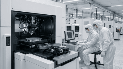
Traditional lithography tools relied on a single wafer stage that handled all functions: loading the wafer, measuring alignment marks, positioning for exposure, and moving between fields. While this approach works at larger nodes, it places competing demands on a single mechanical platform and control loop. Measurement and exposure share the same stage motions and mechanical conditions, which can introduce trade-offs between speed, stability, and accuracy.
Dual stage systems, by contrast, introduce two separate stages within the tool. One stage is typically dedicated to metrology tasks—measuring alignment marks, characterizing wafer geometry, and determining overlay corrections. The other stage focuses on exposure, executing precise, high-speed scanning under optimized conditions. Wafers shuttle between these stages as they progress through the tool.
This architectural shift enables lithography systems to perform alignment and overlay measurements under conditions tailored for accuracy, while exposure scans can be optimized for throughput and focus control, significantly enhancing overall overlay performance.
Core functions of dual stage systems
The dual stage architecture serves several core functions that directly influence overlay accuracy. First, it segregates tasks: the measurement stage concentrates on capturing detailed information about wafer positioning, distortion, and alignment mark locations; the exposure stage focuses on executing the actual patterning with precise motion and focus control.
Second, it enables parallelism. While one wafer is being exposed on the exposure stage, another wafer can be undergoing alignment and overlay measurements on the metrology stage. This parallel processing reduces idle time and allows more extensive measurement without sacrificing throughput.
Third, it supports advanced correction strategies. Data collected on the measurement stage can be used to compute field-by-field or die-by-die overlay corrections, which the exposure stage then applies dynamically during scanning. This tight loop between measurement and exposure is central to achieving nanometer-level overlay performance.
Measurement stage: the overlay information engine
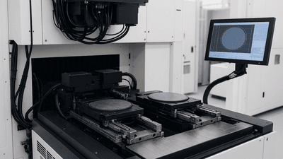
The measurement stage in a dual stage system functions as the overlay information engine. It uses high-precision sensors and optics to locate alignment marks, measure wafer shape and distortion, and characterize how the wafer deviates from ideal geometry. These measurements capture not only global offsets but also local variations across the wafer surface.
Advanced metrology techniques on the measurement stage can include modeling of wafer bow, thermal expansion effects, and process-induced distortions from previous layers. The stage may also detect subtle differences in mark quality or contrast that affect alignment performance. All of this information feeds into overlay models that determine how the exposure should be adjusted.
By performing these measurements on a dedicated stage, the system avoids disturbances from exposure motions and can optimize conditions—such as illumination, focus, and wafer handling—purely for measurement accuracy.
Exposure stage: applying corrections with precision
Once the measurement stage has gathered overlay-relevant data and the system has computed corrections, the exposure stage takes over. Its role is to implement these corrections as the wafer is scanned under the projection optics. The exposure stage must execute precise motions in multiple directions, maintain consistent focus, and manage field-by-field or die-by-die adjustments in real time.
Dual stage exposure platforms often feature sophisticated actuators, position sensors, and control loops designed for ultra-high precision and repeatability. They can apply small shifts, rotations, and scale adjustments to align each exposed field according to the overlay model derived from the measurement stage.
By decoupling exposure motion from measurement tasks, the exposure stage can be tuned strictly for robust, high-speed patterning, while still incorporating the fine corrections needed to achieve overlay targets.
Overlay modeling and correction in dual stage architectures

The interaction between the measurement and exposure stages is mediated by overlay modeling. Using data from the measurement stage, the lithography system builds mathematical representations of how the wafer deviates from the ideal patterning grid. These models capture translations, rotations, magnification differences, and higher-order distortions such as wafer bow or localized stretching.
Dual stage systems often support complex overlay models that vary across the wafer, allowing corrections to be tailored for each field or region rather than relying on simple global shifts. The exposure stage then applies these corrections dynamically, aligning the projected pattern to the modeled wafer geometry.
This modeling-and-correction loop is decisive for overlay accuracy at advanced nodes, where simple corrections are insufficient and non-uniform distortions must be accounted for to maintain alignment within a few nanometers.
Throughput and overlay: resolving the traditional trade-off
Historically, there has been a perceived trade-off between throughput and overlay accuracy. More extensive measurement and correction could improve overlay but at the cost of extra time per wafer, while faster exposure with fewer measurements could boost throughput but degrade alignment. Dual stage systems help resolve this trade-off by enabling parallel operations and dedicated stages.
Because alignment and overlay measurements can be performed on one wafer while another is being exposed, the system gains additional measurement time without extending the overall wafer processing time. This parallelism allows fabs to adopt richer overlay metrology routines and more sophisticated models, improving accuracy without sacrificing throughput.
As a result, dual stage architectures support both high-volume manufacturing and advanced overlay requirements, making them particularly attractive for leading-edge fabs.
Impact on multi-patterning and advanced patterning flows
Multi-patterning techniques, such as double or quadruple patterning, dramatically increase overlay demands because multiple lithography steps must work together to create a single effective pattern. Any misalignment between patterning passes can cause critical dimension variations or pattern collapse.
Dual stage systems play a decisive role in these flows by enabling tight control over overlay between successive patterning exposures. The measurement stage can capture detailed information about how previous patterns lie on the wafer, while the exposure stage uses that data to align new patterns with high precision. Field-by-field corrections help manage small distortions that accumulate over multiple steps.
Without dual stage architectures, achieving the overlay performance needed for complex multi-patterning schemes at advanced nodes would be significantly more difficult, limiting the practical use of these techniques.
3D devices and overlay complexity
Modern devices such as FinFETs, gate-all-around transistors, and 3D NAND add vertical complexity to the overlay equation. Aligning layers in three-dimensional structures requires precise lateral and vertical positioning relative to previously formed features, many of which have non-planar surfaces or buried interfaces.
Dual stage systems support this complexity by enabling more detailed characterization of wafer surfaces and underlying structures through the measurement stage. They can detect shifts or distortions induced by 3D structures and incorporate these into overlay models. The exposure stage then adjusts positioning to account for how vertical features project onto the wafer surface during patterning.
This capability is essential for maintaining overlay accuracy as the industry transitions from primarily planar designs to deeply 3D architectures across both logic and memory.
Tool stability, vibration isolation, and dual stage benefits
Overlay accuracy depends on mechanical stability and vibration control within the lithography tool. Single-stage systems must manage disturbances from all operations—loading, measuring, exposing—on a single platform. Dual stage systems offer more flexibility in isolating and controlling these effects.
The measurement stage can be designed for maximum stability during alignment mark detection, with tailored vibration isolation and motion profiles that minimize mechanical noise. The exposure stage can use optimized scanning trajectories and isolation systems that reduce motion-induced disturbances during patterning.
By allowing each stage to be engineered and tuned for its specific tasks, dual stage architectures reduce mechanical cross-talk and improve overall overlay performance across a wide range of operating conditions.
Software, algorithms, and data use in dual stage systems
Dual stage architectures are supported by sophisticated software and algorithms that manage data flow, compute overlay corrections, and orchestrate stage motions. Alignment data from the measurement stage must be processed quickly and accurately, transforming raw sensor readings into actionable corrections for the exposure stage.
Advanced software can incorporate historical data, machine learning techniques, or model-based predictions to enhance overlay control. For example, patterns of distortions observed in previous lots can inform predictive corrections for new wafers. Dual stage systems provide the structural foundation for such data-driven strategies, since they separate measurement and exposure tasks but maintain a tight integration through shared models.
In this way, dual stage architectures are not just mechanical designs; they are platforms for increasingly sophisticated overlay control algorithms that leverage real-time and historical data.
Implications for fab operations and process integration
For fabs, the adoption of dual stage lithography systems has several implications. Operationally, it allows more flexible scheduling and recipe design. Fabs can choose to increase measurement density or adjust overlay strategies without dramatically affecting throughput, thanks to the parallelism inherent in dual stage architectures.
From a process integration perspective, dual stage systems give engineers more tools to manage overlay across complex flows. Alignment strategies can be tuned for different layers, products, or nodes, and overlay corrections can be tailored to each context. This flexibility supports multi-product fabs and high-mix environments where overlay requirements vary across devices.
Furthermore, the ability to maintain high overlay accuracy across many layers helps fabs push device scaling and integration complexity without hitting immediate alignment limits.
Future trends: beyond dual stages to more advanced architectures
Looking ahead, the role of dual stage systems in overlay accuracy is likely to evolve further. As nodes shrink and devices become more complex, lithography tools may incorporate even more advanced stage architectures, enhanced metrology subsystems, and closer integration with inline overlay measurement tools located outside the scanner.
Potential developments include more granular overlay correction schemes at sub-field levels, tighter coupling between scanner data and external metrology, and increased use of predictive and adaptive algorithms that respond to process variations on the fly. Dual stage systems provide a robust foundation for these trends, and they may be augmented by additional stages or sub-stages dedicated to specialized tasks.
In this trajectory, overlay accuracy becomes an increasingly software-defined and data-driven capability, built on the mechanical and architectural advantages that dual stage systems already provide.
Conclusion: dual stages as decisive overlay enablers
The decisive role of dual stage systems in lithography overlay accuracy stems from their ability to separate, specialize, and integrate measurement and exposure functions. By dedicating one stage to high-precision overlay and alignment metrology and another to optimized exposure scanning, these architectures resolve traditional trade-offs between throughput and accuracy and enable increasingly sophisticated overlay modeling and correction.
As semiconductor manufacturing advances into ever smaller nodes and more complex 3D architectures, the overlay demands placed on lithography systems will only intensify. Dual stage systems stand out as a core enabler of meeting those demands, supporting both high-volume production and the nanometer-level alignment required for next-generation devices. In the broader narrative of lithography evolution, they represent a key step in shifting overlay control from a limiting factor to a managed, highly engineered capability.