Edge Polishing Equipment Opportunities in Growing SOI Substrate Demand
Silicon-on-insulator (SOI) substrates have moved from a niche technology into a mainstream enabler for high‑performance, low‑power, and high‑voltage semiconductor devices. As adoption expands in RF, automotive, power management, and advanced logic applications, demand for SOI wafers is rising steadily. This growth is not just about the active silicon layer and buried oxide quality; it also places new emphasis on wafer edge characteristics, opening a distinct opportunity space for specialized edge polishing equipment.
This blog post explores how growing SOI substrate demand reshapes requirements for wafer edge quality, why edge polishing becomes more critical in this context, and where equipment vendors can position themselves to capture value. It connects device‑level needs to process‑level challenges and outlines the business and technology angles that make edge polishing a promising niche.
SOI substrates: why demand is growing
SOI substrates consist of a thin active silicon layer sitting on top of a buried oxide (BOX) layer and a silicon handle wafer. This structure reduces parasitic capacitance, improves isolation, and enables better control of transistor behavior compared with bulk silicon. As a result, SOI is widely used for RF front‑ends in smartphones, high‑performance processors, and high‑voltage or high‑temperature applications.
Several trends drive growing SOI demand. RF complexity in mobile and wireless systems continues to increase, pushing designers toward SOI for better linearity and isolation. Automotive electronics, including advanced driver‑assistance systems and electrification, need robust devices that operate safely across wide voltage and temperature ranges—roles that SOI often fills. In some advanced logic flows, SOI helps manage leakage and performance trade‑offs.
As these markets expand, wafer suppliers ramp SOI production volumes and broaden their product portfolios, making substrate manufacturing efficiency and yield more important than ever.
Why wafer edges matter more for SOI

Wafer edge quality can affect yield, reliability, and safety in subtle but important ways. Chips are typically placed away from the very edge, but mechanical integrity, particle generation, and stress distributions at the edge impact the whole wafer during processing. For SOI, the multi‑layer structure introduces additional sensitivities.
The interface between the thin active layer, buried oxide, and handle wafer must remain stable and defect‑free. Edge chipping, micro‑cracks, or roughness can create stress concentrators that propagate into active regions during thermal cycling or mechanical handling. Edge defects can also become sources of particles that contaminate critical device areas, especially in high‑aspect‑ratio or high‑sensitivity processes.
As SOI wafers are used in more demanding applications—high frequency RF, safety‑critical automotive systems, advanced sensors—tolerance for edge‑related issues shrinks. This elevates the importance of precise, repeatable edge polishing as part of the substrate manufacturing flow.
Conventional edge processing vs. advanced edge polishing
Traditional wafer edge processing often involves edge grinding to shape and smooth the circumference, followed by simple polishing or cleaning steps to remove debris. For bulk silicon at mature nodes, this level of edge finishing can be sufficient in many cases.
SOI substrates, especially those targeted at advanced nodes or high‑performance applications, require more sophisticated edge treatments. The edge must be formed with controlled geometry, minimal subsurface damage, and tailored surface finish across the layered stack. The goal is to reduce stress, prevent crack initiation, and minimize particle generation during subsequent handling and processing.
This distinction opens room for dedicated edge polishing equipment designed specifically for multi‑layer wafers like SOI, going beyond general‑purpose solutions used for standard bulk silicon.
Key technical requirements for SOI edge polishing

Several technical requirements define effective edge polishing for SOI:
First, damage control: the polishing process must remove micro‑cracks and grinding‑induced defects without introducing new ones. Second, geometry and profile control: edge bevels, radii, and overall shape must meet strict specifications to ensure uniform mechanical and thermal behavior. Third, surface quality: the final edge surface should have low roughness and minimal contamination to reduce particle release and interface perturbations.
Additionally, the process must account for the differential properties of the SOI layers—silicon, oxide, and silicon again—managing selective removal rates and interactions at the interfaces. Achieving all this consistently at high volumes demands specialized equipment, well‑designed tooling, and refined process recipes.
Process integration: where edge polishing fits in the SOI flow
SOI wafers are manufactured through methods such as the Smart Cut process, bonding and thinning, or epitaxial growth on oxide. These flows include steps like wafer bonding, grinding, polishing, and annealing. Edge polishing must be integrated in a way that aligns with these upstream and downstream processes.
Typically, edge shaping and polishing are applied after key bonding and thinning steps, once the multi‑layer structure is established but before final surface finishing and inspection. The edge treatment needs to be compatible with subsequent cleans, CMP, and metrology, and should not compromise the quality of the device surface or buried interfaces.
Equipment solutions that fit seamlessly into existing SOI lines—offering appropriate throughput, footprint, and automation interfaces—will find it easier to gain adoption as substrate suppliers scale their operations.
Yield and reliability benefits: quantifying the opportunity
From the substrate supplier’s perspective, better edge polishing translates directly into yield and reliability benefits. Reduced edge chipping and crack propagation mean fewer wafers lost in later process steps, especially during thermal cycles, handling, and dicing. Lower particle generation at the edge reduces defectivity in device areas, supporting higher yield for downstream customers.
For device makers, SOI wafers with superior edge quality improve process stability, reduce unexpected breakage in tools, and lower the likelihood of random failures originating from edge‑induced stress or contamination. In safety‑critical or high‑reliability applications, such improvements can be essential to meeting qualification standards.
These benefits create a clear economic case: investment in advanced edge polishing equipment can pay back through higher usable yield, fewer customer returns, and stronger substrate performance reputation, particularly as SOI volumes grow.
Market drivers: RF, automotive, and specialty devices
Edge polishing opportunities are tied to the segments most reliant on SOI. RF front‑end modules in smartphones and wireless infrastructure demand high linearity and isolation; they are sensitive to substrate quality and consistency. Automotive electronics require robust substrates that withstand mechanical and thermal shocks over long lifetimes. Power management and specialty analog devices often push voltage and temperature envelopes.
As these segments expand and design win volumes climb, substrate specifications tighten. OEMs and fabless companies may explicitly call out edge quality requirements in their procurement standards. Substrate suppliers that can meet these needs gain competitive advantage; equipment vendors that enable those suppliers tap into the same growth.
Because many of these markets are long‑cycle and safety‑focused, investments made now in edge polishing capabilities can generate returns across multiple product generations.
Equipment design considerations: flexibility and automation
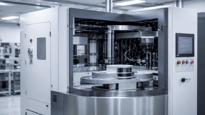
Edge polishing equipment targeting SOI applications must balance flexibility, precision, and productivity. Flexibility is needed to handle different wafer diameters, SOI thicknesses, and stack configurations, including variations in BOX thickness and active layer profiles. Precision is critical for consistent bevel shapes, damage removal, and surface finish at tight tolerances.
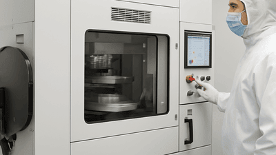
Automation features—robotic wafer handling, integrated inspection stations, recipe management, and data logging—help substrate suppliers scale volume and maintain traceability. Integration with factory MES systems and compatibility with cleanroom standards are essential for high‑volume lines.
Equipment vendors that design edge polishing tools with these considerations in mind can better serve the growing SOI market and differentiate themselves from generic solutions that lack the required specificity and automation depth.
Metrology and inspection: proving edge quality
Advanced edge polishing is only valuable if its results can be measured and verified. Metrology and inspection tools—optical systems, laser profilometers, and defect inspection platforms—must be able to characterize edge geometry, roughness, and damage removal effectiveness.
For SOI, additional attention may be paid to interface behavior near the edge: how the silicon and oxide layers meet, whether there are voids or delamination tendencies, and how these features evolve through thermal cycles. Edge polishing equipment can be paired with in‑line or near‑line metrology to ensure that process drift and tool wear are detected early.
Providing integrated or compatible metrology options enhances the value proposition of edge polishing systems, helping substrate suppliers demonstrate compliance with strict customer specifications and internal quality targets.
Competitive landscape and differentiation
The edge polishing equipment market includes vendors that historically serve bulk silicon wafer producers. As SOI demand grows, these vendors face a choice: adapt their tools and processes to multi‑layer substrates or risk ceding space to more specialized competitors.
Differentiation can occur through several levers: better edge damage removal with minimal material loss, superior edge geometry control across different SOI formats, higher throughput at equivalent quality, and tighter integration with automation and metrology. Vendors that invest early in understanding SOI‑specific challenges—bonded interfaces, BOX performance, and layer thickness interactions—can design tools that address pain points more directly.
Because substrate suppliers may be relatively concentrated compared with downstream device makers, gaining a few key customers can establish a strong position in this niche, creating recurring demand for tools, upgrades, and service.
Environmental and safety aspects
Edge processing involves mechanical removal of material and use of cleaning fluids or coolants. Environmental regulations and safety standards increasingly govern how these operations are conducted. Equipment designed for SOI edge polishing must manage particle collection, slurry or coolant recycling, and operator safety within tightening regulatory frameworks.
Advanced designs may include better containment systems, more efficient filtration, and lower chemical usage, reducing the environmental footprint and operational costs. For customers with strong ESG commitments, such features can influence equipment choices as much as pure technical performance.
Attention to environmental and safety aspects is therefore both a compliance necessity and a potential differentiator for edge polishing solutions aimed at high‑profile markets like automotive and telecom.
Opportunities in 300 mm and future wafer formats
Most SOI production today focuses on standard wafer sizes, with significant activity at 200 mm and 300 mm. As demand for advanced applications grows, 300 mm SOI volumes are likely to rise faster, given their alignment with modern fab infrastructures. Edge polishing opportunities scale in tandem: tools optimized for 300 mm SOI can capture a large share of the high‑volume market.
Potential future wafer formats, including specialized thicknesses or hybrid substrates, may emerge for particular applications. Edge polishing equipment capable of handling such variations without major reconfiguration will offer long‑term flexibility to substrate suppliers, who may need to adapt quickly to new specifications.
Equipment vendors that anticipate these trends in wafer formats and design accordingly can extend their relevance beyond current SOI generations, supporting customers through multiple technology transitions.
Strategic positioning for equipment vendors
For equipment companies, edge polishing in the context of SOI demand represents an attractive opportunity to define a clear niche with strong technical and business logic. Rather than competing head‑on in crowded mainstream equipment categories, vendors can position themselves as key enablers of high‑quality SOI substrates.
Strategic moves may include partnering with major SOI suppliers on co‑development projects, offering pilot tools for new substrate lines, and providing consulting services around edge process optimization. Over time, such relationships can lead to embedded positions in customers’ standard flows, generating recurring hardware and service revenue.
By framing edge polishing not just as a mechanical step but as a yield, reliability, and safety lever, equipment vendors can elevate the perceived value of their offerings and align with the strategic priorities of both substrate suppliers and their end‑customers.
Conclusion: a focused niche with expanding importance
Growing SOI substrate demand in RF, automotive, power, and advanced logic applications is reshaping how wafer quality is defined and controlled. Edge characteristics, once considered secondary, have become key contributors to yield, reliability, and process robustness. In this environment, specialized edge polishing equipment tailored to SOI’s multi‑layer structure and stringent requirements finds a clear opportunity space.
By addressing the technical challenges of damage removal, geometry control, and surface quality—and integrating automation, metrology, and environmental safeguards—equipment vendors can help substrate suppliers meet rising standards and capture expanding markets. As SOI continues its trajectory from niche to mainstream, edge polishing moves from a background task to a strategically important process step, offering a focused but growing arena for innovation and investment in the semiconductor value chain.