ALD Usage Doubles in Advanced Process Nodes
Atomic layer deposition (ALD) has moved from a niche technique to a central pillar of thin-film engineering in leading-edge semiconductor manufacturing. As process nodes advance into ever smaller geometries and more complex three-dimensional architectures, fabs are turning to ALD far more frequently than in previous generations. The statement that “ALD usage doubles in advanced process nodes” captures a real and powerful trend: each node shrink and structural transition typically brings a step-change in how often, and how critically, ALD is used across the flow.
This blog post examines why ALD adoption is accelerating, how its usage expands in logic and memory nodes, what this means for device performance and yield, and how equipment suppliers and fabs are reshaping their strategies to reflect ALD’s rising importance.
From thin-film method to process cornerstone
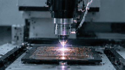
ALD is a thin-film deposition technique based on self-limiting surface reactions. Process gases are pulsed sequentially into a chamber, each reacting with the surface in a way that deposits no more than a single monolayer per cycle. By repeating cycles, engineers build up films with exquisite control over thickness, composition, and uniformity.
Historically, many films in semiconductor devices were deposited using physical vapor deposition (PVD) or chemical vapor deposition (CVD). These methods are fast and cost-effective but can struggle with conformality and precision in extreme aspect ratios or intricate structures. As nodes advanced and structures became more challenging, ALD moved from a specialty tool used for a few critical layers to a mainstream method deployed across multiple steps.
The doubling of ALD usage in advanced nodes reflects this transition: where a previous node might have used ALD sparsely, the newer node introduces ALD at many more points—gate stacks, spacers, liners, barriers, and encapsulation layers.
Why advanced nodes demand more ALD
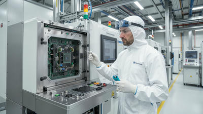
Three primary factors drive increased ALD usage at advanced nodes: geometry, materials, and reliability. First, shrinking feature sizes and higher aspect ratios make it harder for traditional deposition methods to coat surfaces uniformly. ALD’s inherently conformal film growth coats sidewalls and deep trenches evenly, making it ideal for these geometries.
Second, advanced devices rely on complex material stacks—high-k dielectrics, metal gate alloys, diffusion barriers, and engineered interfaces—that must be precisely controlled at the atomic level. ALD excels at atomic-scale thickness control and composition tuning, enabling finely tailored properties.
Third, reliability requirements tighten as operating voltages drop and device densities climb. Defects, pinholes, and thickness variations that were tolerable at larger nodes can become fatal at advanced nodes. By offering smoother, more uniform films, ALD helps meet stringent reliability targets, pushing fabs to adopt it more widely.
ALD in advanced logic: gate stacks and beyond
In advanced logic nodes, gate stacks are a primary driver of ALD adoption. High-k/metal gate (HKMG) technologies often rely on ALD to deposit high-k dielectrics like hafnium oxide and carefully engineered interfacial layers. As gate lengths shrink and gate structures evolve—from planar to FinFETs and nanosheets—the need for uniform, precisely controlled dielectric films becomes acute.
Beyond gate dielectrics, ALD is used for spacers, liners, and barrier layers around the gate and in interconnect structures. For example, ALD can deposit ultra-thin, conformal barriers that prevent copper diffusion in back-end-of-line (BEOL) interconnects, improving electromigration resistance and long-term reliability.
Each new logic node adds complexity to these stacks. The net effect is that ALD appears in more recipe steps, across more layers, and with more criticality. Where older nodes might have used ALD for a few specialized gate layers, cutting-edge nodes integrate it deeply into multiple regions of the device.
ALD in advanced memory: 3D structures and high-aspect ratio features
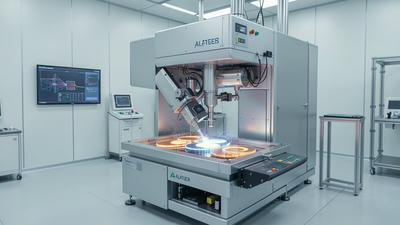
Advanced memory, especially 3D NAND, is another domain where ALD usage has surged. 3D NAND structures stack dozens or even hundreds of layers, with high-aspect-ratio channels etched through the stack. Coating these channels with uniform, thin films is a major challenge for conventional deposition methods.
ALD’s conformal nature makes it the method of choice for many films in 3D NAND: gate dielectrics, channel linings, and certain barrier or spacer layers. As layer counts rise, the number of ALD steps increases, and the total ALD tool hours per wafer grow accordingly.
In DRAM, ALD is used for capacitor dielectrics and electrodes in advanced cell structures. Here too, shrinking geometries and demanding electrical specifications push fabs toward ALD for better control over capacitance, leakage, and variability, adding more ALD steps into the flow.
Vertical and 3D architectures amplify ALD needs
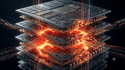
The trend away from purely planar structures toward vertical and three-dimensional architectures magnifies the importance of ALD. FinFETs, gate-all-around (GAA) nanosheets, 3D NAND, and other 3D designs all feature surfaces that are difficult to reach and coat uniformly with line-of-sight techniques like PVD.
ALD’s ability to deposit conformal films on complex topographies makes it practically indispensable for many of these designs. As devices become more 3D, ALD usage per wafer tends to increase, both in number of steps and in process time per step.
The doubling of ALD usage thus mirrors the industry’s broader architectural evolution: as 3D becomes standard, ALD becomes the default method where 2D assumptions about film coverage and uniformity no longer hold.
Material innovation: high-k, metal-nitride, and beyond
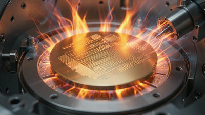
Advanced nodes often introduce new materials or new combinations of known materials. High-k dielectrics, metal nitrides, metal oxides, and tailored multilayers are used to tweak electrical characteristics, reduce leakage, and manage work functions and band alignments.
ALD supports a wide range of chemistries, including metal-organic precursors, halides, and plasma-enhanced reactions. Its ability to deposit complex compounds and alloys in controlled fashion makes it a key tool for material innovation. Engineers can adjust cycle sequences, precursor choices, and plasma steps to fine-tune film properties.
As more nodes lean on material innovation to sustain performance gains, ALD becomes a critical enabler. Each new material stack that joins the process flow often comes with an ALD-based deposition recipe, adding to the overall ALD footprint in advanced manufacturing.
Process control and uniformity: ALD as a yield lever
Yield at advanced nodes depends on controlling variability in critical dimensions, film thickness, and interface quality. ALD provides inherent advantages in process control because each cycle deposits a very predictable amount of material, and growth saturates after one monolayer per cycle.
This self-limiting behavior makes it easier to hit target thicknesses consistently across wafers and lots. It also enhances uniformity across large wafer surfaces and within dense features, reducing local variations that can degrade device performance.
As fabs prioritize yield, they increasingly view ALD as a lever to stabilize and optimize key layers. The decision to replace or supplement other deposition methods with ALD is often justified not only by performance but also by the yield improvements that follow from better-controlled films.
Trade-offs: throughput and cost vs. precision
ALD has real trade-offs. Because films grow one monolayer at a time, ALD processes can be slower than conventional CVD or PVD, especially for thick films. Equipment must handle many precursor pulses and purges, and chamber designs must manage gas flows efficiently to avoid slow cycle times.
From a cost perspective, ALD tools and precursors can be more expensive, and longer process times affect wafer throughput. Fabs therefore apply ALD selectively: where its precision and conformality are truly needed, they accept the cost and throughput penalties; where simpler films suffice, they stick with faster, cheaper methods.
The doubling of ALD usage in advanced nodes reflects a shift in this balance. As more layers become “must have” for ALD due to performance, yield, and 3D geometry requirements, fabs allocate more tool capacity and capital to ALD, even as they continue optimizing for throughput and cost.
Equipment evolution: single-wafer vs. batch ALD, thermal vs. plasma
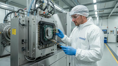
To support increased usage, ALD equipment itself is evolving. Single-wafer ALD tools dominate high-volume, advanced-node logic and memory applications, offering fine-grained process control and integration with cluster tools for in-line processing.
Batch ALD systems remain important for certain applications where throughput and cost per wafer are critical, such as some back-end or specialty layers. Thermal ALD—using only heat to drive reactions—and plasma-enhanced ALD (PEALD), which employs plasma to activate precursors or surfaces, both find roles depending on temperature budgets and film requirements.
As usage doubles, equipment vendors invest in higher-throughput designs, more efficient precursor delivery systems, better chamber cleaning strategies, and smarter process control software. The goal is to make ALD more scalable, reducing its traditional throughput handicap while preserving its precision.
Integration with other process steps
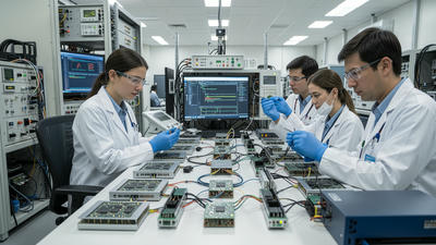
ALD does not exist in isolation; it must be carefully integrated with etch, CMP, implantation, and other steps in the flow. For example, ALD-deposited barriers or liners influence how subsequent etch processes behave, while ALD films may need specific CMP recipes to achieve target planarity without damaging underlying layers.
In advanced nodes, engineers design entire module sequences—deposition, etch, clean, anneal—around material and geometry constraints. As ALD usage increases, these modules must adapt, incorporating ALD’s unique characteristics such as film density, interface chemistry, and surface roughness.
The growing prominence of ALD therefore reshapes integrated process development. Complex modules like gate formation, contact patterning, and 3D memory channel formation increasingly depend on ALD, making it a hub around which other processes are tuned.
Impact on design: knowing ALD is in the toolbox
Device designers and process engineers now assume that ALD is available as a standard tool. This assumption influences design choices. If ALD can reliably deposit uniform, ultra-thin dielectrics on 3D surfaces, designers may choose more aggressive geometries or material combinations than would be feasible with only CVD or PVD.
In turn, this shifts the “design rules” for advanced nodes. Layouts, spacing, and allowable aspect ratios may be set with ALD capabilities in mind. As its usage doubles, ALD’s presence in the toolbox expands the feasible design space for logic and memory, enabling architectures that might otherwise be impractical.
In this way, increased ALD usage becomes not just a manufacturing trend but a design enabler, opening paths to performance and density gains via novel structures and stacks.
Supply chain and precursor markets
The doubling of ALD usage also affects upstream supply chains. Precursor suppliers that provide metal-organic compounds, halides, and other ALD-specific chemistries see rising demand as fabs consume more precursors per wafer and per layer.
These suppliers must ensure high purity, consistent reactivity, and stable supply, as precursor variations can cause film defects or process drift. Supply chain resilience becomes more important; disruptions in precursor markets could directly affect ALD availability and fab output.
As ALD usage grows, collaborations between equipment vendors, precursor suppliers, and fabs intensify, focusing on co-developing chemistries and hardware that deliver better films at higher throughput and lower cost.
Looking forward: will ALD keep growing at this pace?
The question is whether ALD usage will continue doubling with each major node transition or eventually plateau. As nodes approach physical and economic limits in traditional scaling, the industry’s reliance on 3D and heterogeneous integration suggests that ALD’s role will remain strong.
However, ALD growth may evolve from simply “more layers” to “more sophisticated applications,” including selective ALD, area-specific deposition, and integration into advanced packaging flows. Selective ALD, for instance, could deposit films only where needed, further changing module designs and potentially reducing etch complexity.
For now, the trend is clear: advanced nodes bring more ALD steps, deeper integration, and greater strategic importance. It is reasonable to expect ALD to remain a central focus of process innovation, with equipment and chemistry advances supporting continued expansion of its footprint.
Conclusion: ALD’s doubling usage reflects a deeper shift
The doubling of ALD usage in advanced process nodes is more than a statistic; it reflects a deeper shift in how semiconductors are designed and manufactured. As geometries shrink and architectures turn 3D, the need for conformal, precisely controlled films makes ALD indispensable across gate stacks, interconnects, and memory structures.
While throughput and cost challenges remain, the benefits in performance, yield, and reliability have driven fabs to weave ALD into more steps and modules at each new node. For equipment vendors, material suppliers, process engineers, and designers, ALD has become a primary lever of progress—a sign that the future of scaling depends as much on atomic-level film engineering as on transistor geometry alone.