Challenges for Back-End Test Equipment (Probers/Handlers) in Massive AI Chips
Massive AI chips—large, power‑hungry accelerators packed with billions of transistors and complex interconnect fabrics—have rapidly become central to data centers, cloud platforms, and high‑performance computing systems. Their front‑end design and fabrication attract much attention, but back end test is just as critical. Probing and handling these devices at wafer sort and final test is significantly more challenging than for traditional logic or consumer chips, because AI devices push the limits of size, power, thermal behavior, and interface complexity.
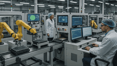
This blog post explores the key challenges that back end test equipment—especially probe cards, probing stations, and device handlers—face when testing massive AI chips. It looks at mechanical and electrical constraints, thermal and power issues, parallel test strategies, reliability concerns, and the evolving demands that AI architectures place on existing back end infrastructure.
Massive AI chips: what makes them different
AI accelerators and large data center chips differ from conventional devices in several ways. They often have very large die sizes, complex multi‑core or multi‑tile architectures, and wide high‑bandwidth memory interfaces. Many operate at high currents and power densities during realistic workloads, and they may integrate advanced packaging features such as interposers or chiplets.
From a test perspective, this means more pins or contacts, wider buses, and more intricate test modes. It also means that realistic performance testing involves stressing devices with demanding power and thermal conditions. The back end test equipment that interfaces with these chips must therefore handle larger footprints, higher pin counts, and more intense operating environments than traditional handlers and probe systems were originally designed for.
These differences set the stage for the specific challenges that probes and handlers encounter when AI devices move through the test flow.
Probe cards: scaling to large die and high pin count
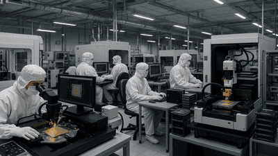
Probe cards physically connect test equipment to wafer‑level devices during sort. Massive AI chips often have large die areas and many I/O pads for data, control, and power. Probe cards must cover this area with sufficient contact points, maintaining alignment accuracy and consistent contact quality across a wide footprint.
Scaling probe cards to such dimensions introduces mechanical challenges: maintaining planarity across the card, ensuring that all probes touch with appropriate force, and avoiding bow or warping that could cause uneven contact. High pin counts also complicate routing within the card, increasing complexity and potential signal integrity issues.
Designers must balance mechanical robustness, electrical performance, and manufacturability, often pushing probe card technology to the edge of what existing materials and fabrication techniques can support.
Contact reliability and pad wear
Reliable contact between probes and device pads is essential for accurate measurements. Massive AI chips may use smaller pads, denser pad arrays, or specialized pad metallization to support high‑speed interfaces. Probing must achieve clean, repeatable contact without damaging these pads or introducing debris.
Repeated probing can cause pad wear or micro‑damage, especially at high contact forces or with certain probe tip geometries. In AI devices where many test insertions are needed, cumulative wear becomes a concern. Probe cards must be designed to minimize pad damage while still penetrating oxide or contamination layers enough to ensure good electrical contact.
Managing this trade‑off—durability versus gentleness—is a core challenge, particularly when test strategies aim for high parallelism and throughput.
Power delivery and IR drop during wafer sort
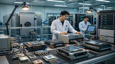
AI chips draw substantial current under load, even during test patterns designed to exercise core logic and memory. At wafer sort, supplying these currents through probes and probe cards can create significant IR drop, voltage variation, and thermal stress in the contact and routing structures.
Probe cards and test equipment must provide robust power delivery networks capable of handling high currents without excessive voltage sag or localized heating. Designers may need thicker conductors, more power probes, or dedicated power delivery structures within the card. At the same time, they must preserve signal integrity for high‑speed signals sharing the card.
Balancing these demands is harder for massive AI chips than for lower‑power devices, making power delivery a critical design and operational challenge in back end test.
Signal integrity at high bandwidth interfaces
Massive AI chips rely on wide, high‑speed interfaces: internal buses, memory links, and external connections to systems or interposers. Testing these interfaces at speed requires that the probe card and test setup maintain signal integrity—low jitter, controlled impedance, minimal crosstalk—along the entire path from tester to device.
High pin counts and dense routing on probe cards increase the risk of signal degradation. Longer trace lengths and complex layer stacks can introduce reflections, skew, and coupling. As data rates rise, traditional probe card designs may struggle to meet signal integrity requirements, especially across large die footprints.
Addressing this challenge often involves advanced materials, careful PCB stack‑up design, controlled impedance routing, and possibly the use of embedded circuitry or local termination on the card itself.
Thermal management at wafer sort
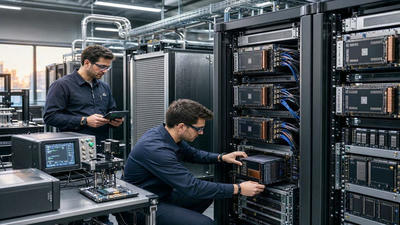
Power‑dense AI devices generate significant heat, even during test operations that may not fully replicate worst‑case workloads. At wafer sort, this heat must be managed without dedicated package‑level heatsinks or system cooling. Prober chucks and thermal control systems must remove heat from the wafer while maintaining stable, controlled temperature conditions.
Probes and probe cards contribute to thermal dynamics; they can create local hotspots or provide thermal paths. If device temperature is not controlled, test results may vary, and devices might experience thermal stress beyond intended limits. Advanced probe systems incorporate sophisticated chuck cooling, temperature monitoring, and sometimes active thermal management features to keep AI devices within acceptable operating ranges.
Managing thermal behavior becomes more complex when multiple large AI dies are tested in parallel on a wafer, amplifying the overall heat load on the prober.
Handlers: dealing with large and heavy packages
At final test, device handlers must physically move packaged chips between test sockets and buffers. Massive AI chips often come in large, complex packages—multi‑chip modules, interposer‑based packages, or high‑pin‑count BGA and LGA formats. These packages can be heavier, taller, and more mechanically sensitive than typical consumer chips.
Handlers must be designed to grip, transport, and align these packages without damage or misalignment. Socket insertion forces and mechanical tolerances become more demanding. Larger packages may require modified handler tooling, stronger actuators, and more precise positioning systems. At the same time, handlers must maintain high throughput in high‑volume test environments.
This combination of physical complexity and performance requirements challenges traditional handler designs and pushes development of specialized equipment tailored for AI device formats.
Socket design and contact reliability in final test
Socket design for massive AI chips is itself a major challenge. High pin counts, fine pitches, and mixed‑signal interfaces require sockets with precise contact geometry, robust spring structures, and materials that can handle repeated insertions without losing performance. Thermal considerations also matter: sockets must allow effective heat transfer to the handler’s thermal management systems.
Contact resistance stability over time is critical for accurate test measurements. For AI chips, small variations in supply and signal levels can affect performance, so socket contacts must remain stable across many cycles. Wear, contamination, and material aging can degrade contacts, requiring careful materials selection and maintenance strategies.
Designing sockets that balance durability, thermal performance, signal integrity, and ease of maintenance is a non‑trivial task, particularly as AI devices push pin counts and power levels upward.
Parallel test versus power and thermal limits
Test throughput is driven by parallelism: testing many devices simultaneously in multi‑site setups. For massive AI chips, parallel test is attractive but constrained by power and thermal limits. Testing multiple high‑power devices at once can exceed the capacity of test power supplies, socket designs, or handler cooling systems.
Back end test engineers must balance site count against power and thermal headroom. In some cases, they may reduce parallelism to maintain safe operating conditions, sacrificing throughput to protect device integrity and measurement quality. In others, system upgrades—stronger power supplies, enhanced cooling, or more efficient test patterns—are needed to sustain multi‑site operation.
This trade‑off is more acute for AI devices than for lower‑power chips, impacting test economics and equipment utilization strategies.
Test time, vector volume, and equipment utilization
Massive AI chips often require complex test programs with large vector volumes. Functional tests, memory tests, high‑speed interface checks, burn‑in or stress tests, and characterization routines can all be lengthy. Longer test times per device reduce overall throughput and increase demands on equipment utilization and scheduling.
Probe stations and handlers must support extended test durations without compromising mechanical stability, thermal control, or contact reliability. Equipment downtime becomes more costly when each device occupies test resources for longer periods. Improving test efficiency—optimizing vector sets, using built‑in self‑test features, and prioritizing critical test coverage—helps, but hardware and test setup must also accommodate long test cycles.
These issues put pressure on back end equipment to deliver higher reliability and availability, as any failure or instability during a long test can waste significant time and resources.
Reliability and maintenance of probes and handlers
Heavy usage, high power, and complex mechanical motions increase wear on probes, probe cards, sockets, and handlers. For AI chips, where test conditions are more demanding, equipment components may reach end‑of‑life faster or require more frequent maintenance. Probe tips can wear or accumulate debris; sockets may lose spring tension; handler mechanisms can experience higher mechanical stress from large packages.
Maintaining high reliability under these conditions requires robust preventive maintenance programs, spare parts strategies, and sometimes redesigns of critical components. Equipment suppliers and fabs must work together to monitor performance, identify failure modes, and schedule maintenance in ways that minimize disruption to test operations.
This reliability challenge is not only technical but also logistical, affecting staffing, spare inventories, and off‑line qualification processes for replacement components.
Adapting existing test floors to AI devices
Many test floors were originally designed around typical logic, memory, or mixed‑signal devices, not massive AI accelerators. Introducing AI chips into these environments can expose infrastructure gaps: insufficient power delivery, inadequate cooling, handlers that cannot handle large packages, or probe systems that struggle with large die sizes.
Fabs and OSATs must evaluate how well their existing equipment can accommodate AI devices and where upgrades or new tools are required. In some cases, creative adaptations—custom fixtures, improved airflow, better power management—can extend the utility of existing systems. In others, dedicated test cells designed specifically for AI devices may be needed.
Adapting test floors involves both capital decisions and operational changes, including retraining staff and revising test planning and scheduling practices.
Emerging solutions and innovation in back end equipment
The challenges of testing massive AI chips are driving innovation in back end equipment. Probe card manufacturers are developing new materials and architectures to improve planarity, power delivery, and signal integrity for large, high‑pin‑count devices. Prober vendors are enhancing thermal control, chuck capabilities, and alignment systems to handle heavier wafers and more demanding test conditions.
Handler and socket suppliers are creating solutions tailored to large AI packages, with improved mechanical robustness, better cooling integration, and optimized contact structures. Test systems themselves are evolving, with stronger power supplies, advanced thermal management modules, and software features that help manage long, complex test programs.
These innovations respond directly to AI‑driven demands and will likely spill over into improved capabilities for other high‑performance devices as well.
Strategic implications for test strategy and cost
Testing massive AI chips is inherently more complex and resource‑intensive than testing smaller, lower‑power devices. This has strategic implications for test cost and strategy. Companies must decide how much test coverage is necessary at wafer sort and final test, which parameters can be monitored through built‑in self‑test, and how to balance test thoroughness against throughput and cost.
Investments in advanced probes, handlers, and test infrastructure must be justified by the value of catching defects early and ensuring reliable, high‑performance devices in the field. For high‑margin AI products used in critical data center or AI workloads, the cost of insufficient testing can be much higher than the added expense of robust back end equipment.
As a result, back end test for AI chips tends to be seen not as a cost center to be minimized, but as a strategic capability that protects brand, customer trust, and long‑term system performance.
Conclusion: back end equipment at the frontier of AI hardware
Massive AI chips push the boundaries of semiconductor technology, and back end test equipment—probes, probe cards, handlers, and sockets—must keep pace. Large die sizes, high pin counts, intense power and thermal conditions, and complex interfaces create a suite of challenges that traditional tools were not originally designed to handle.
Addressing these challenges requires innovation across mechanical, electrical, and thermal domains, as well as close collaboration between equipment suppliers, fabs, and test engineers. As AI devices become more pervasive and powerful, the decisive role of robust, capable back end test equipment will only grow, ensuring that the chips driving the AI revolution meet their performance and reliability promises before they ever reach real‑world systems.