Tracking Expansion Plans of Japan’s Semi Material Giants: Sumitomo, Mitsubishi, Shin-Etsu
Japan’s semiconductor materials sector has long been a quiet powerhouse beneath the global chip industry. From wafers and photoresists to specialty gases, CMP consumables, and packaging materials, Japanese firms anchor critical parts of the supply chain for fabs worldwide. Among these firms, Sumitomo, Mitsubishi, and Shin Etsu stand out as “semi material giants” whose strategies and expansion plans shape both regional ecosystems in Japan and global availability of key inputs.
This blog post discusses how expansion planning typically looks for these companies, why their moves matter so much to the semiconductor industry, which material segments are likely focal points, and how fabs and policymakers should think about their evolving footprints. It does not rely on confidential project details or speculative announcements, but rather on the structural logic that tends to guide expansion decisions for large Japanese materials groups.
Japan’s role in semiconductor materials
Japan’s materials sector covers a broad spectrum of semiconductor inputs. Local firms supply silicon wafers, photoresists, advanced CMP consumables, leadframes and substrates, encapsulants, bonding wires, and numerous high-purity chemicals and gases. Fabs around the world depend on these materials for front-end and back-end processes, especially at advanced nodes where quality and consistency requirements are highest.
The concentration of expertise in Japan—combining precise manufacturing, strong chemistry and materials science, and long relationships with major device makers—gives companies like Sumitomo, Mitsubishi, and Shin Etsu a central role in global capacity planning. Their expansions or constraints can ripple through tool utilization, fab ramps, and localization efforts in other regions.
Understanding their typical expansion logic helps clarify where future bottlenecks or relief may appear.
Sumitomo: diversified materials and targeted expansions
Sumitomo-affiliated materials businesses tend to operate across multiple semiconductor-related segments: CMP slurries and pads, packaging materials, resins, and various specialty chemicals. Expansion planning for such a diversified player usually focuses on segments where demand growth is structurally strong—advanced-node CMP, high-performance packaging, and specialized polymers for lithography and etch-related processes.
Sumitomo’s expansions are typically characterized by incremental capacity adds and technology upgrades rather than sudden, speculative builds. Plants may be debottlenecked, lines duplicated, or new modules added to support specific customers and nodes. R&D facilities often expand in parallel, backing new formulations and materials tuned to emerging logic and memory processes.
In practice, this means fabs can expect Sumitomo to align its growth with clear demand signals from leading-edge and high-volume customers, while maintaining disciplined investment patterns.
Mitsubishi: chemicals, gases, and integration
Mitsubishi’s materials footprint spans high-purity chemicals, electronic gases, and various industrial inputs that feed semiconductor fabs. Expansion plans for such portfolios tend to focus on strengthening supply for key regional fab clusters—both in Japan and abroad—and on upgrading purity and specifications to match advanced-node requirements.
Typical expansion moves include new or enlarged purification plants for acids and solvents, gas separation and purification facilities, and bulk supply infrastructure near major fabs. Mitsubishi may also integrate upstream and downstream operations more tightly, for example linking basic chemical production with electronic-grade refinement and on-site distribution capabilities.
Through these moves, Mitsubishi aims to reduce logistics risk, improve responsiveness to customer ramps, and support higher purity grades needed for ultra-clean processes, while maintaining strong safety and environmental performance.
Shin Etsu: wafers and strategic materials capacity
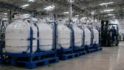
Shin Etsu is widely associated with silicon wafers and a range of other semiconductor-related materials. Wafer capacity planning is particularly critical because it directly underpins fab output. Expansion strategies typically revolve around adding new crystal pulling, slicing, polishing, and epitaxy capacity, often in phases aligned with demand forecasts for 200 mm and 300 mm wafers and for specific node ranges.
Shin Etsu’s wafer expansions usually emphasize quality and stability over sheer volume. Investments are made to support stringent flatness, defect density, and dopant uniformity requirements at advanced nodes. Additional capacity may also be devoted to specialty wafers—such as SOI or high-resistivity substrates—if demand justifies it.
Beyond wafers, Shin Etsu’s moves in other materials (such as certain resins or specialty chemicals) follow a similar pattern: targeted capacity additions combined with ongoing process optimization to ensure consistent, high-spec supply for top-tier fabs.
Drivers behind expansion: demand, technology, and risk
Expansion plans for Sumitomo, Mitsubishi, and Shin Etsu are typically driven by three forces: demand growth, technology shifts, and risk management. Demand growth comes from increased wafer starts, more complex process flows, and broader use of advanced nodes in logic, memory, and specialty devices. As each wafer consumes more materials—whether in CMP, lithography, or cleaning—materials suppliers see sustained volume growth opportunities.
Technology shifts—such as new device architectures, more layers, and strict purity needs—motivate investments in upgraded plants and new formulations. These expansions often focus on enabling specific process modules: advanced CMP for deep interconnect stacks, ultra-clean chemicals for sensitive gate stacks, or high-spec wafers for cutting-edge nodes.
Risk management involves reducing exposure to single-site production, improving regional balance, and enhancing resilience against disruptions, earthquakes, or logistics bottlenecks. Plants may be duplicated or distributed across multiple locations to support continuity.
Regional balance: domestic versus overseas capacity
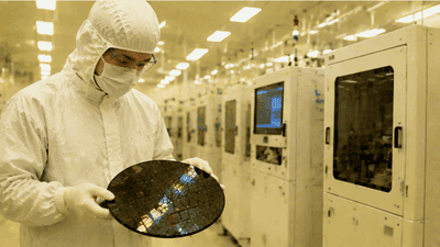
Japan’s material giants increasingly balance domestic capacity with overseas facilities. Domestic plants often serve as technology centers, focusing on high-end products and close collaboration with Japanese fabs. Overseas expansions typically support major fab clusters in other regions, providing local supply, shorter lead times, and compliance with regional regulation.
For Sumitomo and Mitsubishi, this may mean chemical and gas plants in multiple continents, each tailored to nearby customers and environmental standards. For Shin Etsu, wafer plants and related facilities may be distributed to serve international foundries and IDMs more efficiently.
This global spread of capacity reflects a dual strategic intent: maintain Japan as a core R&D and manufacturing hub, while ensuring that global customers have access to reliable local or regional material supplies.
Technology-node focus in expansion planning
Materials expansions are rarely node-neutral. Capacity planning often targets specific technology ranges: mature nodes for automotive and industrial chips, mid-range nodes for mobile and consumer SOCs, and leading-edge nodes for high-performance logic and memory. Sumitomo’s CMP and packaging materials, Mitsubishi’s chemicals and gases, and Shin Etsu’s wafers may all be mapped to particular node bands.
When demand for advanced nodes rises faster, expansions may prioritize high-spec materials suited for those nodes, such as ultra-flat wafers, high-purity chemicals with lower metal content, or CMP systems designed for narrow lines and complex stacks. Conversely, strong mature-node demand from power electronics and automotive can justify expansions in more traditional materials with reliability rather than extreme scaling as the primary design driver.
Tracking which nodes expansions target helps fabs and downstream suppliers anticipate where capacity may tighten or relax over the next few years.
Cost, capital intensity, and investment discipline
Material plants for semi applications are capital-intensive. Wafer manufacturing equipment, chemical purification lines, gas separation units, and CMP production facilities all require substantial upfront spending. Japanese material giants typically adopt disciplined investment approaches: expansions phased, tied to clear customer commitments, and built with long service horizons in mind.
This discipline means capacity growth tends to lag short-term spikes in demand but align well with sustained structural trends. It reduces the risk of overcapacity, which can destabilize pricing and profitability. In return, fabs gain relatively stable, predictable material supply curves rather than boom-and-bust patterns.
Understanding this cautious capital logic helps explain why announcements of large new plants or big capacity jumps are relatively rare and usually backed by strong industry-level signals.
Supply-chain resilience and redundancy
Recent global disruptions have underscored the importance of resilient supply chains. For Sumitomo, Mitsubishi, and Shin Etsu, expansion plans often include building redundancy and backup capacity. Multiple plants may produce similar materials, providing fallback options if one facility experiences issues. Critical steps—such as high-purity distillation or wafer polishing—may be distributed across sites with shared standards.
Redundancy does not eliminate risk but reduces the chance that a single incident will significantly affect global supply. Fabs and equipment makers increasingly discuss resilience explicitly with material suppliers, influencing where and how new capacity is added.
Japan’s material giants, with their scale and long experience, are in a strong position to invest in such redundancy while maintaining efficiency.
Environmental, safety, and regulatory considerations
Expanding chemical, gas, and wafer facilities requires careful attention to environmental and safety regulations. Japanese companies have long experience meeting strict domestic standards on emissions, waste treatment, and workplace safety. New plants or upgrades must comply with these rules and, for overseas sites, with local regulations.
Modern expansions increasingly incorporate sustainability measures: energy-efficient equipment, reduced waste streams, improved recycling of solvents or chemicals, and careful management of hazardous materials. Such investments may raise upfront costs but can improve long-term risk profiles and align with global ESG expectations.
For customers, working with material suppliers that prioritize environmental and safety performance can be an important part of corporate responsibility and risk mitigation strategies.
Interaction with localization policies outside Japan
Many regions are pursuing semiconductor localization policies, including efforts to build domestic material supply chains. Japan’s semi material giants must navigate this trend carefully. On one hand, their expertise and product portfolios make them attractive partners for localized production plans. On the other, they must maintain their own strategic control and technology leadership.
Typical responses include joint ventures, technology licensing, and regional manufacturing investments that localize some production while keeping core R&D and critical know-how centralized. Sumitomo, Mitsubishi, and Shin Etsu can thus participate in localization initiatives in North America, Europe, or other parts of Asia while continuing to anchor global materials innovation from Japan.
Such moves shape not only their own expansion footprints but also the broader geography of semiconductor materials supply.
Customer collaboration and co-development
Expansion plans are rarely made in isolation. Japan’s material giants engage in co-development programs with major fabs, foundries, and IDMs, sharing roadmaps and aligning material capabilities with process needs. New wafer specifications, CMP chemistries, or high-purity chemicals may be co-designed around upcoming nodes or device types.
These collaborations influence where and how capacity is expanded. Plants may be built near key customers or configured to produce specific formulations tied to joint development outcomes. Long-term supply agreements and technology partnerships provide financial and strategic anchors for such investments.
For fabs, close collaboration with Sumitomo, Mitsubishi, and Shin Etsu can secure access to tailored materials and early insight into expansion trajectories that affect their own manufacturing plans.
Risks and uncertainties in expansion paths
Despite the structured nature of expansion planning, risks remain. Demand projections can shift due to macroeconomic changes, policy developments, or technological disruptions. New materials may prove more challenging to industrialize than expected, delaying capacity ramps. Regulatory changes or unforeseen events can affect plant construction or operation.
Japanese material giants typically manage these uncertainties by building flexibility into their expansions—modular plants, adaptable lines, and staged investments that can be accelerated or slowed. They also maintain diversified portfolios so that weakness in one segment can be offset by strength in another.
Fabs and downstream partners should recognize these uncertainties and monitor not just headline expansion announcements, but also actual ramps and performance over time.
What fabs and policymakers should watch
Fabs focusing on long-term capacity planning should watch several signals in the expansion behavior of Sumitomo, Mitsubishi, and Shin Etsu: new wafer plant announcements and upgrades, chemical and gas purification facilities near key fab clusters, and CMP and packaging material capacity additions aligned with advanced packaging and interconnect trends.
Policymakers interested in supply-chain resilience and industrial strategy should monitor the geographic distribution of these expansions, the degree of domestic versus overseas investment, and the level of integration with local fabs and research institutions. These patterns indicate how deeply Japanese material giants are intertwining with regional semiconductor ecosystems.
For both groups, understanding the incremental and disciplined nature of these expansions is essential to setting realistic expectations and planning complementary investments.
Conclusion: Japan’s material giants as strategic anchors
Sumitomo, Mitsubishi, and Shin Etsu occupy strategic positions in the semiconductor materials landscape. Their expansion plans—wafers, chemicals, gases, CMP consumables, and more—quietly but decisively shape the capacity and resilience of fabs around the world. While specific project details evolve over time, the underlying logic is consistent: align with structural demand, support advanced-node and specialty technologies, and manage risk through disciplined, globally balanced investment.
For an industry increasingly aware of material bottlenecks and supply-chain vulnerabilities, tracking how these Japanese giants expand offers valuable insight into future constraints, opportunities, and the evolving geography of semiconductor manufacturing. Their role as semi material anchors will remain central as the world builds the next generation of chips and the infrastructure that supports them.