2026 Global Wafer Shipment Area YoY Growth Forecasts: Divergence and Consensus
As the semiconductor industry moves through 2026, expectations for global wafer shipping area growth sit at the core of many strategic decisions. Year‑on‑year (YoY) wafer area forecasts influence how wafer manufacturers plan capacity, how fabs schedule expansions and technology migrations, and how equipment and materials suppliers shape their own production plans. Yet the forecasts themselves are far from uniform. Different institutions—industry bodies, market research firms, banks, and corporate strategists—offer projections that diverge meaningfully in magnitude and composition, even when they point in broadly similar directions.
This blog post explores that mix of divergence and consensus. It looks at how different players frame 2026 global wafer shipping area growth, which assumptions drive the spread in views, where forecasts converge despite differing methodologies, and what this means for companies that must make real‑world decisions under imperfect visibility. The aim is not to endorse specific numbers, but to clarify the underlying logic shaping the landscape of 2026 wafer area expectations.
What wafer shipping area represents—and why YoY growth matters
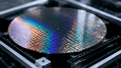
Wafer shipping area is a standardized way of measuring how much wafer capacity moves through the supply chain, typically reported in terms of total square centimeters or equivalent units shipped over a period. Because wafers come in different diameters and are used across multiple technology nodes, aggregate area provides a more comparable metric than raw wafer counts.
Year‑on‑year growth in shipping area reflects changes in global demand for manufacturing capacity. When area grows, it implies either higher output volumes, broader utilization of existing lines, or the addition of new capacity. When growth slows or turns negative, it signals digestion phases, inventory corrections, or structural shifts. For 2026, wafer area growth forecasts are central to understanding whether the industry is in a robust upturn, a cautious expansion, or a more subdued phase driven by selective strength in certain segments.
Because wafer area connects upstream wafer manufacturers with downstream fabs, equipment suppliers, and materials vendors, its projected trajectory has wide‑ranging implications.
Sources of divergence in 2026 forecasts

Divergence in 2026 wafer shipping area forecasts arises from the different lenses through which institutions view the industry. Some emphasize macroeconomic trends, projecting wafer demand based on broad GDP, consumer spending, and industrial output indicators. Others anchor their models in specific semiconductor end markets—smartphones, PCs, automotive, data centers—and extrapolate wafer requirements from chip demand in each category.
Differences also emerge from how strongly analysts weigh structural drivers like AI workloads, electrification of vehicles, and industrial automation. Bullish views often assume these drivers will outweigh lingering inventory adjustments or economic caution, leading to robust wafer area growth. More conservative views see AI and electrification as important but still partially offset by softness in traditional consumer electronics or slower IT spending recovery.
These varying assumptions create a spread of expected YoY growth rates, even when analysts agree that 2026 will be healthier than preceding trough years.
Consensus: broad recovery from prior corrections
Despite disagreements on magnitude, there is notable consensus on direction. Most institutions expect 2026 global wafer shipping area to grow compared with the low points that followed the last major inventory correction and cyclical downturn. The rationale is that inventory levels in key markets have normalized sufficiently for new orders to reflect genuine end demand rather than stock clearing.
Consensus also exists around the idea that structural drivers—cloud expansion, AI training and inference, automotive semiconductors, and industrial control—will underpin baseline wafer requirements across both advanced and mature nodes. Even cautious forecasts typically assume positive growth, though they may favor single‑digit rates and modest acceleration rather than a sharp surge.
This directional consensus provides a common foundation: while the exact YoY percentage might differ, most players agree that 2026 wafer area is moving up, not down.
Logic versus memory: different growth stories

One of the key friction points in 2026 wafer area forecasts lies in the relative contributions of logic and memory. For logic and foundry wafers, many institutions expect steady or strong growth driven by ongoing node migrations and demand for processors in AI, mobile, and general computing. These wafers tend to support high‑value chips and remain central to data center and consumer device roadmaps.
Memory wafers—especially DRAM and NAND—have historically seen more pronounced cycles. Analysts diverge on how aggressively memory makers will expand wafer area in 2026. Some foresee disciplined, gradual increases aligned with long‑term demand growth and pricing recovery; others anticipate more robust ramps to prepare for future AI and data‑intensive workloads.
The balance between logic and memory growth assumptions plays a large role in determining overall wafer shipping area forecasts, particularly because memory capacity expansions can shift area figures significantly when they occur.
Mature nodes versus advanced nodes: where growth concentrates
Forecast divergence also reflects differing views on node mix. Mature nodes—covering power devices, analog, microcontrollers, display drivers, and many automotive chips—use large fractions of global wafer area. Some institutions believe that these segments will see continued expansion in 2026 as electrification, safety systems, and industrial automation broaden demand for robust, proven technologies.
Others argue that recent capacity investments in mature nodes have created enough headroom, meaning 2026 growth will be more modest as the industry digests earlier additions. In contrast, advanced nodes for leading‑edge logic and certain memory applications are widely expected to grow in wafer area, but from a smaller base and often concentrated in a limited number of fabs.
Different assumptions about how much mature‑node area expands versus stabilizes contribute to the spread of overall wafer shipping area growth forecasts, especially because mature nodes account for substantial absolute area even when their percentage growth rates are moderate.
Regional differences: where area growth is expected

Institutions also diverge in how they break down growth by geography. Some models project strong wafer shipping area growth tied to new or expanding fabs in regions emphasizing industrial policy and manufacturing onshoring—such as North America and parts of Europe and Asia. These forecasts assume significant incremental area from new capacity coming online or ramping.
Others anticipate that a large portion of 2026 area growth will still come from established manufacturing centers, including East Asian regions with long‑standing wafer production bases. They see policy‑driven new fabs contributing, but not yet dominating global area increases within a single year.
This regional uncertainty interacts with technology‑mix assumptions: where new fabs are focused on mature nodes or specialized segments, their impact on overall advanced‑node area might be limited, even as total area rises.
Inventory and utilization: how much idle capacity remains
Another axis of divergence is the perceived level of existing idle or underutilized capacity going into 2026. Institutions that believe there is still substantial idle capacity at certain nodes or in specific regions tend to project lower wafer shipping area growth, reasoning that improved utilization—not new area—is sufficient to meet demand.
Conversely, those who see most installed capacity either well‑utilized or structurally mismatched to emerging demand (for example, too much capacity at nodes with fading relevance) forecast higher wafer area growth to reflect the need for new lines tuned to current and future product mixes.
These differences often stem from how analysts interpret utilization data, fab guidance, and product roadmaps, and they directly impact estimates for the incremental area required in 2026.
Consensus elements: AI, automotive, and industrial demand
Despite the spread in numbers, there is notable consensus around certain demand drivers. AI and high‑performance computing are widely acknowledged as major contributors to wafer area needs, particularly at advanced logic nodes and for high‑bandwidth memory devices. Automotive electronics—including powertrain control, ADAS, and infotainment—are consistently seen as steady or growing drivers at mature and mid‑range nodes.
Industrial and automation applications, along with power electronics for energy infrastructure, also appear frequently in institutional narratives as structural supports for wafer area growth. These sectors are viewed as less volatile than consumer devices and more linked to long‑term investment cycles, helping underpin wafer demand even when traditional consumer segments fluctuate.
This shared recognition of structural drivers forms the consensus backbone of 2026 wafer shipping area expectations, even as quantitative forecasts differ.
Methodological differences: top‑down versus bottom‑up
Forecasting methodologies contribute substantially to divergence. Top‑down approaches start from macro variables and end‑market predictions, translating broad demand trends into implied wafer area. These models may smooth volatility and emphasize long‑term correlations between economic indicators and semiconductor activity.
Bottom‑up approaches begin with fab‑specific plans, announced capacity expansions, technology migrations, and known ramp schedules. They aggregate expected wafer starts across facilities and convert these into shipping area projections. Such models can capture detailed project timelines but may be sensitive to changes in individual companies’ plans.
Institutions that lean heavily on one method or the other produce forecasts that reflect their chosen lens. Top‑down models might under‑ or over‑estimate area if structural shifts break historical patterns, while bottom‑up models might miss unannounced changes or macro‑driven adjustments to capex plans.
Implications for wafer manufacturers
For wafer suppliers, the mix of divergence and consensus in 2026 forecasts has practical consequences. Consensus on positive growth supports planning for moderate capacity increases, debottlenecking existing lines, and targeted investments in new facilities or diameter conversions. Divergence in actual growth magnitude, however, encourages caution in deploying capital too aggressively.
Wafer manufacturers may choose flexible strategies: adding capacity in phases, focusing on segments with strongest structural demand, and maintaining options to scale up or down as more data emerges during the year. They often monitor real‑time orders and inventory trends while using external forecasts as boundary conditions for best‑ and worst‑case planning.
This approach allows them to benefit from growth opportunities without over‑extending in an environment where forecast dispersion remains significant.
Implications for fabs and equipment suppliers
Fabs and equipment makers also rely on wafer area forecasts to shape their strategies. For fabs, expected area growth informs decisions about adding new lines, upgrading existing capacity, and choosing which nodes to expand. Divergent forecasts may lead them to prioritize modular, scalable capacity additions and to build more flexibility into their node mix plans.
Equipment suppliers, particularly those serving front‑end processes, interpret wafer shipping area growth as a proxy for demand for many tool types. Strong forecast growth suggests sustained orders for lithography, etch, deposition, CMP, clean, and metrology, especially where node mix is skewed toward their key segments. Forecast dispersion, however, motivates a diversified product and regional portfolio, balancing exposure to advanced and mature nodes and different geographies.
Both fabs and equipment firms increasingly supplement external forecasts with direct customer dialogues and internal scenario analysis, using wafer area expectations as one input among several.
Using divergence as a planning tool
Rather than treating forecast divergence as purely problematic, many companies use it explicitly in planning. By comparing optimistic, base‑case, and conservative wafer area projections for 2026, they build scenario frameworks that test their strategies against multiple potential outcomes.
For example, a wafer manufacturer might plan core capacity increases that are justified under conservative growth assumptions, with optional expansion steps if actual demand tracks closer to bullish forecasts. A fab might line up equipment orders and facility options that can be accelerated or delayed depending on how wafer area trends materialize in the first half of the year.
In this way, divergence becomes a measure of uncertainty that informs risk management, rather than a source of paralysis.
What consensus and divergence mean for 2026 and beyond
Looking at 2026 as a whole, the coexistence of consensus and divergence in global wafer shipping area forecasts paints a nuanced picture. On one hand, there is broad agreement that the industry is past the deepest part of its last correction and is moving into a phase of renewed growth, supported by structural demand across multiple sectors. On the other, meaningful uncertainty remains about how strong that growth will be and how it will be distributed across nodes, regions, and product categories.
For stakeholders, the key takeaway is less about betting on a single number and more about understanding the logic behind different projections. Appreciating why some institutions are more aggressive or cautious, and how their assumptions relate to one’s own business exposure, is more valuable than fixating on any particular percentage figure.
As the year unfolds and real shipment data accumulates, forecasts will converge or adjust. But the underlying forces—AI, electrification, industrial digitization, policy‑driven capacity shifts—will continue to shape wafer shipping area trajectories beyond 2026, making today’s mix of divergence and consensus a crucial reference point for long‑term strategy.