The Material System Transition of Sputtering Targets (Al/Cu/Ti/Co) in Advanced Interconnects
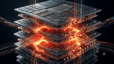
Advanced interconnects have quietly become one of the most challenging frontiers in semiconductor manufacturing. As device performance, power efficiency, and reliability demands tighten at each new logic and memory node, the wiring that connects transistors and functional blocks has evolved just as dramatically as the transistors themselves. Central to this evolution is the material system used in thin-film deposition, especially sputtering targets based on aluminum (Al), copper (Cu), titanium (Ti), and cobalt (Co). The transition in these target materials reflects a broader shift in how the industry manages resistance, electromigration, barrier integrity, and manufacturability in increasingly complex interconnect stacks.
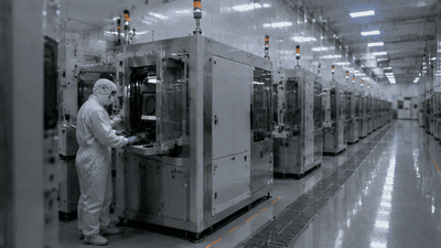
This blog post explores the material system transition of sputtering targets in advanced interconnects. It looks at how Al, Cu, Ti, and Co have been used over time, why their roles are changing, what drives the adoption of new combinations and alloys, and how these shifts impact tool requirements, process integration, and supply chains.
Interconnect scaling: from simple wiring to complex stacks
In earlier technology nodes, interconnects were relatively straightforward: a limited number of metal layers, larger feature sizes, and moderate concerns about resistance and electromigration. Aluminum was widely used due to its ease of processing, established toolsets, and acceptable performance for the era’s speeds and densities.
As nodes shrank and clock frequencies increased, interconnect delay emerged as a major performance limiter. The industry responded by introducing copper to reduce resistance, adding barrier and liner layers to manage diffusion and reliability, and increasing the number of metal levels to accommodate complex routing. Modern interconnects now feature multi-level stacks, low-k dielectrics, intricate via structures, and carefully engineered metals and interfaces.
Within this landscape, sputtering targets for Al, Cu, Ti, Co, and their alloys play key roles in forming conductive lines, barrier layers, seed layers, and capping films that collectively define interconnect behavior.
Aluminum: the early workhorse and its limitations
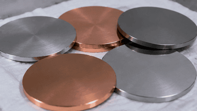
Aluminum was the dominant interconnect material in earlier generations because it was relatively easy to deposit, pattern, and etch. Sputtering tools designed for Al provided robust, high-throughput deposition, and the industry had extensive experience with Al-based metallization.
However, Al’s resistivity and electromigration behavior became problematic as feature sizes shrank and current densities rose. The higher resistance contributed to timing delays, while electromigration risk increased at narrow widths and high currents. These limitations set the stage for copper’s introduction as a lower-resistance alternative.
While Al has not disappeared entirely—it remains relevant in some niche and backend applications—the material system transition for advanced interconnects is defined by the shift toward Cu and more complex barrier and capping schemes.
Copper: lower resistance, higher integration complexity
Copper’s lower resistivity made it attractive for reducing interconnect delay and power consumption at advanced nodes. Its adoption brought significant performance benefits, enabling higher-speed logic and more efficient routing. Sputtering targets for copper became central to deposition of seed layers and certain liner or cap structures.
Yet copper introduced its own challenges. It diffuses readily into surrounding dielectrics, potentially degrading device performance and reliability. Direct etching of copper is difficult, leading the industry to adopt damascene processes: patterning trenches and vias in dielectrics, then filling them via deposition and CMP. Copper’s integration therefore required barrier layers, seed films, and carefully controlled deposition and planarization steps.
As nodes advanced, the interplay between Cu and barrier/cap materials—many of which are deposited by sputtering—became one of the most critical aspects of interconnect engineering.
Titanium: adhesion, barriers, and interface control
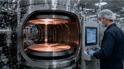
Titanium has long been used in interconnect stacks as an adhesion layer, diffusion barrier component, and interface engineering material. Ti sputtering targets enable deposition of thin films that improve metal adhesion to underlying dielectrics or other metals and help control interfacial properties.
In copper damascene flows, Ti or Ti-based alloys may be used in combination with other barrier materials to form composite layers that restrict Cu diffusion while maintaining acceptable resistance. Ti can also appear in liners or contact structures where robust adhesion and controlled reactions are needed.
As interconnect stacks become more complex, Ti’s role is often tuned: thickness, composition, and sequencing are adjusted to optimize both reliability and electrical performance, making Ti targets part of a nuanced material system rather than a simple standalone solution.
Cobalt: emerging player in advanced interconnects
Cobalt has emerged as a key material in advanced interconnect systems, particularly at nodes where traditional copper-based schemes face increasing constraints. Cobalt’s properties—such as better electromigration resistance in certain geometries and favorable behavior in narrow lines and vias—make it attractive for specific layers and structures.
Cobalt sputtering targets are used to deposit films that serve as liners, barriers, or even primary conductors in selected portions of the interconnect stack. In some advanced nodes, cobalt has been explored or adopted for middle-of-line contacts or certain segments of local interconnects where its reliability advantages outweigh its higher resistivity compared with bulk Cu.
The introduction of Co into the material system represents a strategic trade-off: leveraging superior reliability and electromigration resistance in tightly scaled features while carefully managing resistance and process complexity.
Composite and alloy targets: tailoring properties
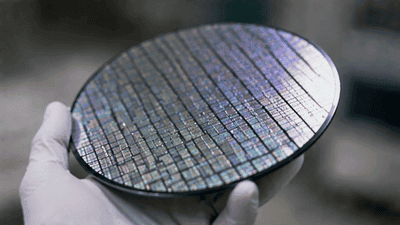
Modern interconnect engineering often relies on composite and alloyed sputtering targets rather than pure elements alone. Combining Al, Cu, Ti, Co, or other metals in specific ratios can yield films with tuned properties: improved adhesion, controlled grain structure, modified resistivity, or enhanced barrier performance.
Alloy targets allow deposition of multi-component films in a single sputter step, simplifying integration and improving uniformity across the wafer. For example, Ti-based alloys may be tailored to balance barrier effectiveness and electrical behavior, while Co-containing alloys can adjust stress and reliability characteristics.
This trend toward alloy and composite targets reflects the complexity of advanced interconnects: simple materials rarely meet all requirements, so engineered combinations become the norm.
Thickness scaling and the role of barriers and liners
As interconnect lines and vias shrink, the relative thickness of barriers and liners becomes more significant. Thick barriers consume cross-sectional area, raising resistance; thin barriers risk insufficient diffusion control and reliability issues. Sputtering targets for Ti, Co, and other barrier materials must support deposition of ultra-thin, uniform films that satisfy both constraints.
Advanced sputter processes aim to deposit conformal barriers and liners with minimal thickness while preserving integrity. This requires precise control over target composition, sputtering parameters, and chamber conditions. The material system transition toward optimized Ti and Co-based barriers reflects the need to balance competing demands in ever-narrower features.
The interplay between Cu conductors and Ti/Co barriers and liners is therefore a central focus of interconnect scaling strategies.
Electromigration and reliability as design drivers
Electromigration—mass transport of metal atoms under high current densities—has become a primary reliability concern in advanced interconnects. As lines narrow and currents remain high, the risk of void formation and open circuits increases. Material selection and interface design are critical levers for mitigating this risk.
Sputtering targets for Cu, Co, and related materials are chosen and engineered with electromigration behavior in mind. Film microstructure, grain boundaries, and interfaces influence how atoms move under stress. Cobalt and certain Co-containing films can offer improved electromigration resistance in specific geometries, prompting their use where reliability margins must be widened.
The material system transition thus reflects not just electrical performance but long-term reliability, with sputtering targets playing a key role in shaping film behavior at the atomic scale.
Resistance: managing the RC delay problem
Interconnect resistance and capacitance together determine RC delay, which impacts signal timing and overall chip performance. Copper’s low resistivity helps, but as wires shrink and roughness or barrier contributions become more significant, effective resistance can rise. Material choices for liners, caps, and even the conductor itself directly affect this trend.
Sputtering targets for Cu and alternative conductor materials must support films with low resistivity, controlled grain orientation, and minimal scattering effects. Meanwhile, barrier and liner targets must enable films thin enough to reduce resistance impact but robust enough for diffusion control. In some contexts, cobalt-based or other materials are used in ways that optimize overall RC performance, even if their intrinsic resistivity is higher than Cu, due to improved geometry or reduced barrier overhead.
Balancing RC delay is another driver behind the evolving Al/Cu/Ti/Co material system in advanced interconnects.
Integration with low-k dielectrics
Advanced interconnects rely on low-k dielectrics to reduce capacitance and improve RC performance. However, low-k materials can be mechanically and chemically fragile, making integration with metal stacks more challenging. Sputtered films from Al, Cu, Ti, and Co targets must adhere well, avoid damaging the dielectric, and maintain interface stability over time.
Barrier and liner materials often serve as protective interfaces between metals and low-k dielectrics, absorbing stress and controlling reactions. Ti and Co-containing films are frequently engineered to meet these roles, with sputtering processes tuned to minimize damage and contamination.
The material system transition thus involves not only electrical and reliability considerations but also complex mechanical and chemical compatibility with advanced dielectrics.
Tool and process implications of target changes
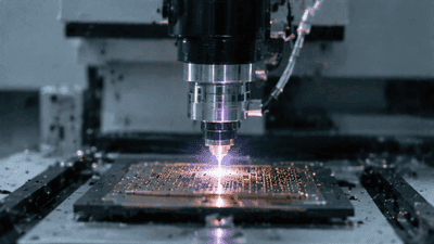
Changes in sputtering target materials affect tool design, process recipes, and maintenance. Different metals and alloys sputter with distinct rates, angular distributions, and plasma characteristics. Chambers may need modified power delivery, magnet configurations, or gas mixtures to accommodate new targets while maintaining film quality.
Target life, erosion patterns, and particle generation can vary with material, influencing tool uptime and defectivity. Co and Ti-based targets may require more stringent contamination controls or specialized handling compared with Al or Cu. As material systems evolve, equipment vendors and fabs collaborate to refine tool configurations and process windows for each target type.
This integration work is essential: without stable, repeatable sputter processes, the theoretical advantages of new interconnect materials cannot be realized in production.
Supply chain and localization of sputtering targets
The transition in sputtering target materials also has supply chain implications. Producing high-purity Al, Cu, Ti, Co, and alloy targets requires specialized metallurgical processes, precise alloying control, and rigorous quality assurance. As advanced interconnects rely more heavily on specific compositions and structures, demand for sophisticated targets grows.
Regions investing in semiconductor localization often view sputtering targets as strategic materials, seeking domestic production capabilities to reduce dependency on imported metals and target fabrication. Localization initiatives may focus first on Cu and Al targets, then extend to Ti and Co alloys as capabilities mature.
Ensuring reliable target supply is critical: any disruption in advanced-node sputtering materials can quickly affect interconnect production and, by extension, chip output.
Future directions: beyond Al/Cu/Ti/Co
While Al, Cu, Ti, and Co dominate current discussions, future interconnects may introduce additional metals or alloys as nodes advance and new architectures emerge. Ruthenium and other metals are being explored in some contexts for contacts or specific interconnect layers. Novel barrier materials and engineered multi-layer stacks could further complicate the material landscape.
Sputtering targets will evolve to include these new compositions, continuing the trend toward more complex, tailored materials. The criteria for adoption will remain similar: improved reliability, manageable resistance, compatible integration with dielectrics and existing processes, and feasible supply chains.
As such, the material system transition seen in Al/Cu/Ti/Co today may represent an ongoing, iterative journey rather than a final destination.
Conclusion: material systems as a cornerstone of advanced interconnects
The transition in sputtering target material systems—from Al-centric to more complex combinations of Cu, Ti, Co, and alloys—captures the essence of advanced interconnect evolution. As wiring structures become smaller, more layered, and more critical to device performance and reliability, the metals and barriers that form them must meet increasingly stringent demands.
Sputtering targets sit at the center of this transformation, enabling the deposition of films that control resistance, electromigration, diffusion, adhesion, and compatibility with low-k dielectrics. For fabs, tool makers, and material suppliers, understanding and managing this material system transition is essential to sustaining progress at advanced nodes and preparing for the next generation of interconnect challenges.